
Plasma etching method

a technology of etching and plasma, applied in the direction of electrical discharge tubes, decorative arts, electrical apparatus, etc., can solve the problems of increasing power consumption, mask shoulder, and increasing power consumption, and achieves accurate formation, high throughput, and economization of power consumption.

Inactive Publication Date: 2006-07-27
TOKYO ELECTRON LTD
View PDF7 Cites 34 Cited by
  • Summary
  • Abstract
  • Description
  • Claims
  • Application Information

AI Technical Summary

Benefits of technology

The present invention provides a plasma etching method for accurately rounding the shoulder portion of a recess in a silicon substrate, while also controlling the radius of curvature of the edge portion of the upper sidewall constituting the recess. The method includes a first plasma process of forming deposits on the etching target layer at least around the boundary between the mask layer and the etching target layer, followed by a second plasma process of etching the etching target layer. The second plasma process rounds off the edge portion of the upper sidewall constituting the recess. The method can be applied to trench etching in a shallow trench isolation process and can control the leakage current between the gate electrode and the active area, leading to economization of power consumption. The plasma etching apparatus includes a plasma supply source, a processing chamber, a supporter, a gas exhaust unit, a gas supply unit, and a controller for controlling the plasma etching apparatus. The control program can be executed on a computer for controlling the plasma processing apparatus.

Problems solved by technology

However, recently, with the trend of requirement for high integration and high speed of LSI (large scale integrated circuit), a design rule of semiconductor devices forming the LSI is getting finer and, at the same time, economization of power consumption is increasingly required.
As a result, a leakage current between a gate electrode and an active area through the shoulder portion increases, thereby causing a problem that power consumption becomes increased.
Since, however, it is a multi-step plasma etching method involving the first step of forming a shallow trench by plasma etching the silicon substrate, the second step and the third step, a shoulder of a mask may be damaged due to a prolonged etching time and, thus, a further improvement is required to enhance an accuracy of microprocessing.

Method used


Image

  • Plasma etching method
  • Plasma etching method
  • Plasma etching method

Examples


Embodiment Construction

[0025] Hereinafter, a preferred embodiment of the present invention will be described with reference to the accompanying drawings.

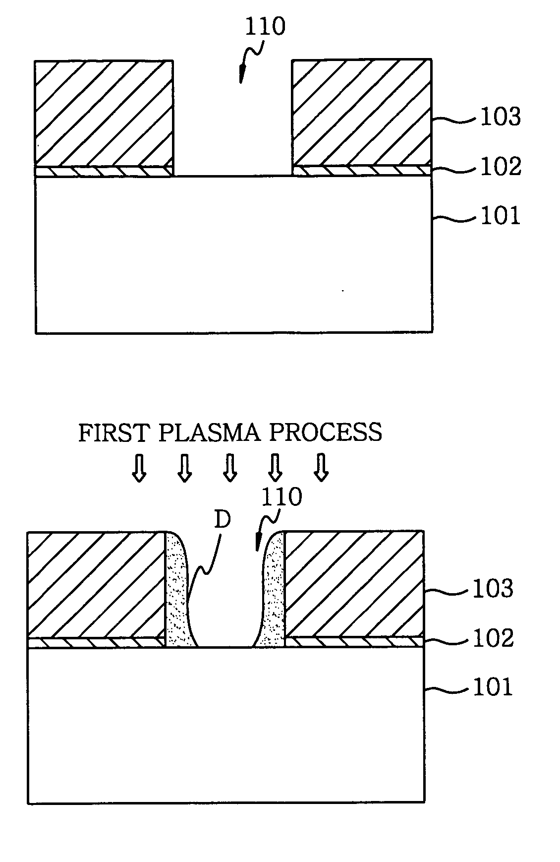
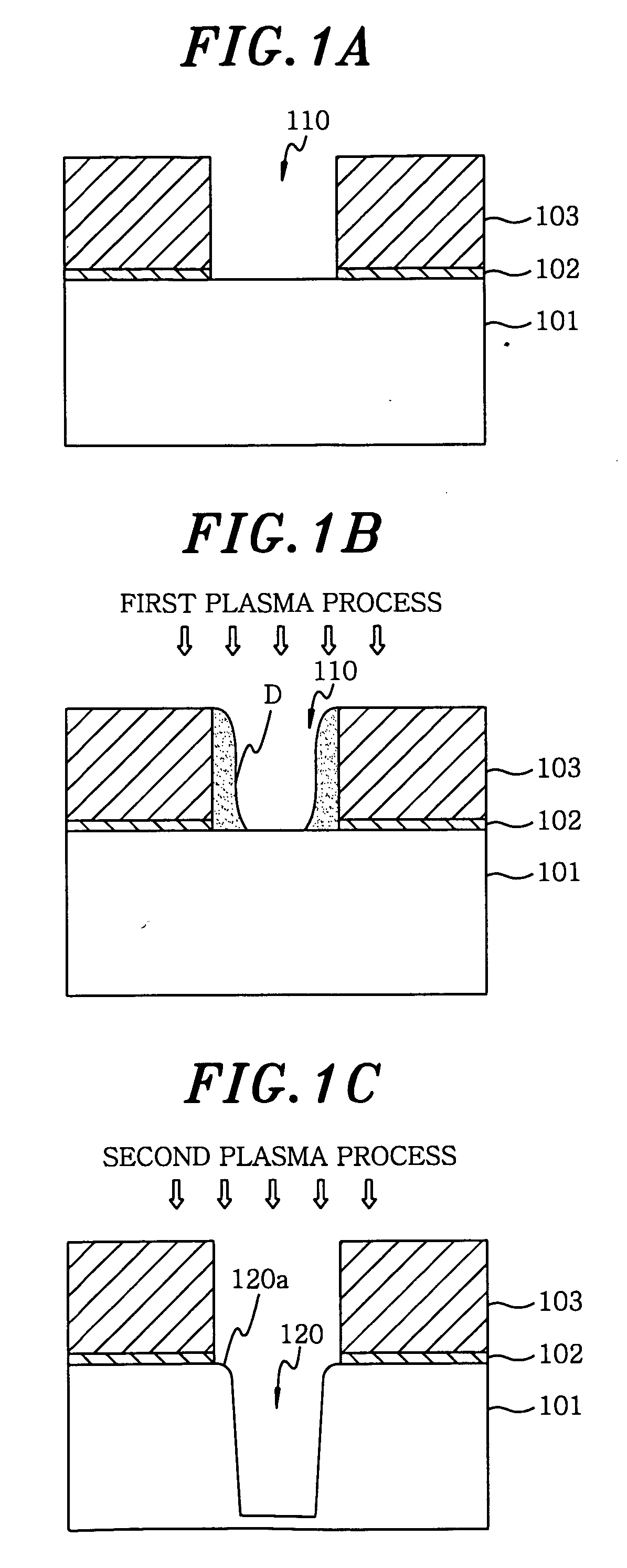
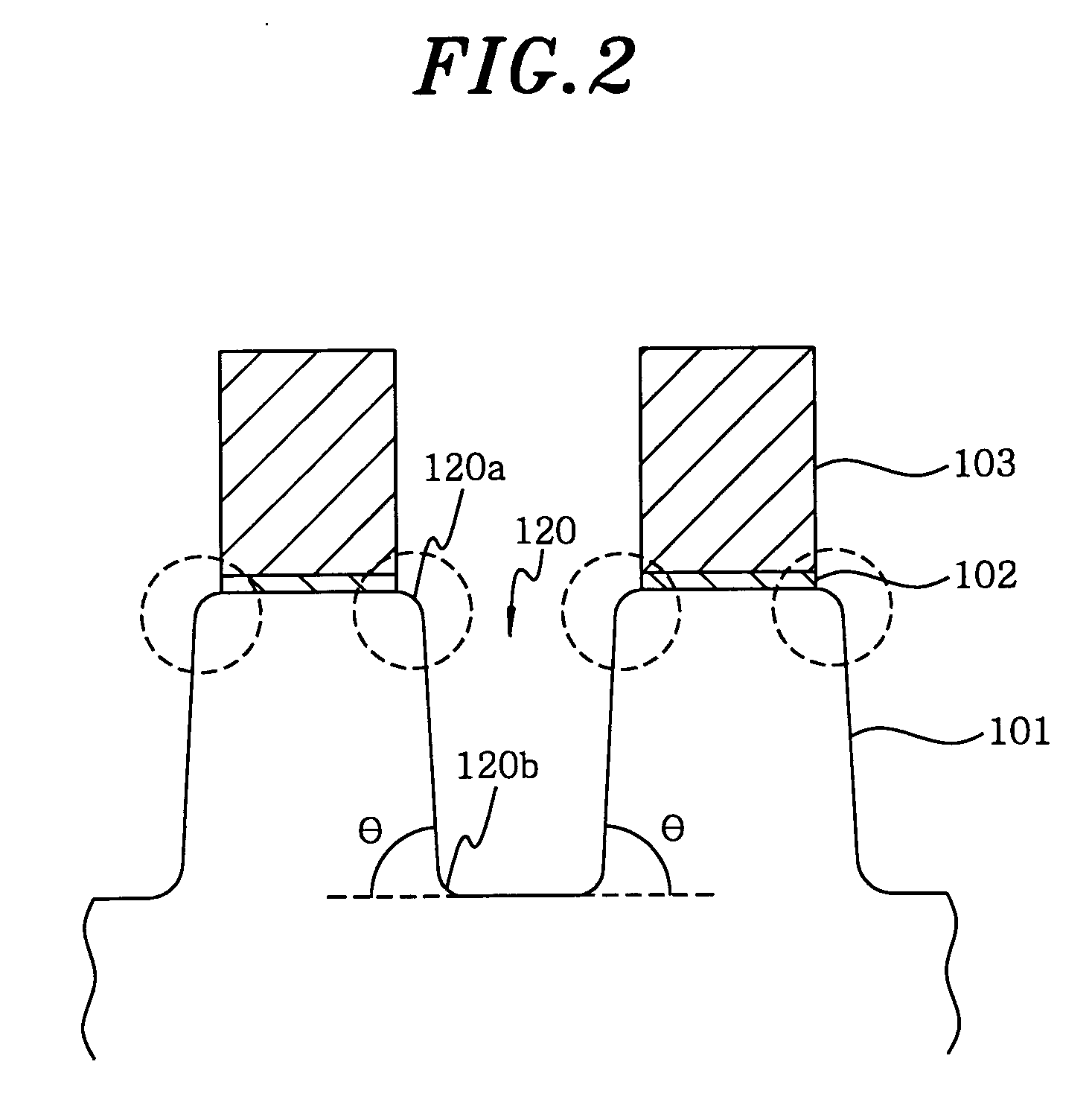
[0026]FIGS. 1A to 1C schematically show enlarged longitudinal cross sectional views of principal parts of a semiconductor wafer W (hereinafter, simply referred to as “wafer”) in a silicon trench etching process in the STI or the like to explain the preferred embodiment of the present invention. As shown in FIG. 1A, the wafer W includes a silicon substrate 101; a silicon oxide film 102 such as SiO2 formed on the silicon substrate 101; and a silicon nitride film 103 such as Si3N4 formed on the silicon oxide film 102. The silicon nitride film 103 serves as a hard mask.

[0027] The silicon nitride film 103 and the silicon oxide film 102 are patterned after a predetermined shape, and form a mask layer. FIG. 1A shows a groove portion 110 serving as an opening portion of a pattern. Further, a process of patterning the silicon nitride film 103 and the silicon oxi...


PUM

PropertyMeasurementUnit
processing timeaaaaaaaaaa
angleaaaaaaaaaa

Abstract

A plasma etching method for etching an object to be processed, which has at least an etching target layer and a patterned mask layer formed on the etching target layer, to form a recess corresponding to a pattern of the mask layer in the etching target layer, includes a first plasma process of forming deposits on the etching target layer at least around a boundary between the etching target layer and the mask layer in an opening portion constituting the pattern of the mask layer, and a second plasma process of forming the recess by etching the etching target layer after the first plasma process. An edge portion of an upper sidewall constituting the recess is rounded off in the second plasma process.

Description

CROSS-REFERENCE TO RELATED APPLICATIONS [0001] This document claims priority to Japanese Patent Application Number 2005-13911, filed Jan. 21, 2005 and U.S. Provisional Application No. 60 / 650,962, filed Feb. 9, 2005, the entire content of which are hereby incorporated by reference.FIELD OF THE INVENTION [0002] The present invention relates to a plasma etching method; and, more particularly, to a plasma etching method applicable to, e.g., trench formation in a shallow trench isolation (STI) that is a device isolation technique in a manufacturing process of a semiconductor device. BACKGROUND OF THE INVENTION [0003] An STI has been known as a technique for electrically isolating a device formed on a silicon substrate. The STI involves the sequential steps of etching a silicon substrate through a mask of, for example, a silicon nitride film to form a trench therein; filling the trench with an insulating film such as SiO2; and planarizing the substrate by chemical mechanical polishing (CM...

Claims


Application Information

Patent Timeline
Patent Type & Authority Applications(United States)
IPC IPC(8): C23F1/00H01L21/306H01L21/302B44C1/22C03C15/00
CPCH01J37/32935H01L21/3065H01L21/3086
Inventor SHIMIZU, AKITAKAOKA, HIROMI
Owner TOKYO ELECTRON LTD
Learn More