Measuring method and measuring system for measuring the imaging quality of an optical imaging system

a technology of optical imaging and measuring system, which is applied in the direction of microlithography exposure apparatus, instruments, measurement devices, etc., can solve the problems of long exposure time, high equipment and time cost, and the degree to which the quality of the products produced is determined and limited, etc., to achieve fast and precise measurement of projection objectives, low cost, and low complexity

Inactive Publication Date: 2006-01-05
CARL ZEISS SMT GMBH
View PDF4 Cites 26 Cited by
  • Summary
  • Abstract
  • Description
  • Claims
  • Application Information

AI Technical Summary

Benefits of technology

[0012] It is one object of the invention to provide a measuring method and a measuring system which permit a high-precision measurement of optical imaging systems at the site of use thereof with a low outlay in respect of time and a low complexity in respect of apparatus. It is another object to enable a fast and precise measurement of projection objectives in microlithography projection exposure apparatuses of various designs.
[0024] In one development, provision is made of a sensor unit, which encompasses the reference structure and the recording medium with positionally correct spatial assignment with respect to one another. If the sensor unit is arranged in such a way that the reference structure essentially coincides with the image surface, then the recording medium is at the same time also arranged positionally correctly, e.g. at a distance behind the reference structure parallel to the latter. The sensor unit may be dimensioned and shaped in such a way that it can be introduced instead of an object to be exposed, such as a wafer, into a mount provided for said object. The sensor unit may for example essentially have the slice form of a wafer and be incorporated in place thereof into a wafer stage and be demounted again after the measurement. In this way, in a projection exposure apparatus, at the site of use thereof, it is possible to change between production configuration (for wafer exposure) and measurement configuration in a simple manner. All that is necessary for this purpose besides changing the sensor unit instead of the wafer is to bring a suitable measuring structure into the region of the object plane, e.g. by exchanging the reticle with the useful pattern, said reticle being used for the wafer exposure, for a measuring mask carrying the two-dimensional mask structure of the measuring system. A platform-independent measuring system is thus created.
[0029] In multiple fringe methods, that is to say in methods with a carrier frequency having been set, the spatial resolution plays an important part in the detection of spatial intensity distributions of a superimposition pattern since the phase angles are calculated from relative positions of the fringe positions of fringes. The phase information is thus coded as a lateral offset of fringes. In electronic cameras that are currently available, pixel sizes of up to approximately 6-7 μm are typically achieved, which corresponds to a resolution of approximately 70-80 line pairs per mm. If, by contrast, the information coded in the superimposition pattern is detected by means of a suitable spatially continuous recording medium, for example a suitable film or a photoresist layer, then resolutions of 400 lp / mm or more can readily be achieved even with typical standard materials. The higher spatial resolution capability and the absence of discretization of the information (non-pixelation) of film material and other continuous recording media is thus an advantage, precisely for the multiple fringe methods, over acquiring information with the aid of a CCD camera.
[0030] The measuring system may have a very compact, simple construction in the region of the reference structure. All parts required here may be combined in a sensor unit encompassing a reference substrate for carrying the reference structure and a recording carrier for carrying and / or supporting the recording medium. The reference substrate may be a plate made of a transparent material, in the case of which the reference structure is fitted to or in the vicinity of a plate surface. The recording carrier may likewise be a plate made of a transparent material and carry and / or support the recording medium on one of its plate surfaces. The reference substrate and the recording carrier may be formed by a single common plate of suitable thickness, which may essentially have the form of a wafer. It is also possible for the reference substrate and the recording carrier to be separate elements, for example two plates, which, if appropriate, can be brought into optical contact with one another along complementary contact surfaces, e.g. by wringing, and can be separated from one another. This embodiment enables a method variant in which the recording carrier is separated from the reference substrate after the measurement of the imaging system with the aid of the sensor unit. While the reference substrate with the possibly sensitive reference structure can remain at its location, the recording carrier can be brought to an evaluation device and the recording medium can be evaluated there. This reduces the risk of damage to the possibly expensive and sensitive reference substrate during different process steps and said reference substrate can be multiply reused. The recording carrier that carries the recording medium is generally less sensitive and can be provided inexpensively. The recording carrier may be a flexible film that carries the recording medium. The film can be pressed, adhesively bonded or fixed in some other way onto a planar or curved supporting surface for the recording and be removed after the recording.

Problems solved by technology

The finer the structures to image, the greater the degree to which the quality of the products produced is determined and limited by imaging errors of the optical imaging systems used.
However, since a large part of the illumination light is masked out at the special reticle, extremely long exposure times result for the wafer.
The evaluation of the exposed wafer is costly in respect of apparatus and time.
The method is time-consuming.

Method used


Image

  • Measuring method and measuring system for measuring the imaging quality of an optical imaging system
  • Measuring method and measuring system for measuring the imaging quality of an optical imaging system
  • Measuring method and measuring system for measuring the imaging quality of an optical imaging system

Examples


Embodiment Construction

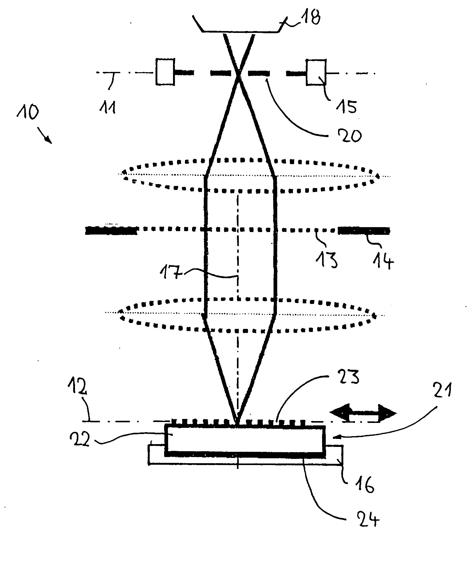
[0056] The invention is explained in more detail below using the example of the measurement of projection objectives for microlithography; however, it is also suitable for the measurement of other optical imaging systems, for example of photooptics or the like. FIG. 1 schematically shows a projection objective 10 designed for imaging with ultraviolet light, said projection objective being incorporated into a projection exposure apparatus (not illustrated) in the form of a wafer stepper at the production site of a semiconductor chip manufacturer. The projection objective 10 serves for imaging a pattern—arranged in its object plane 11—of a reticle provided with a useful pattern into the conjugate image plane 12 with respect to the object plane, on a reduced scale without an intermediate image. A semiconductor wafer covered with a photoresist layer is situated there. Located between object plane and image plane are a plurality of lenses, two of which are shown by dashed lenses, and a p...


PUM


Abstract

In a measuring method for measuring the imaging quality of an optical imaging system (10), a measuring mask is provided, which has a mask structure (20), which can be arranged in the region of an object surface of the imaging system. Furthermore, provision is made of a reference structure (23) adapted to the mask structure, which reference structure is to be arranged in the image surface (12) of the imaging system, and a two-dimensionally extended, radiation-sensitive recording medium (24), which is arranged in a recording position in such a way that a superimposition pattern that arises when the mask structure is imaged onto the reference structure can be detected by the recording medium. For the evaluation of the recording medium, the recording medium is brought from the recording position into an evaluation position remote therefrom. The measuring method and the associated measuring system are particularly suitable for fast, high-precision measurement of projection objectives in the incorporated state in microlithography projection exposure apparatuses.

Description

[0001] This application is a continuation application of international patent application PCT / EP02 / 14559, filed on Dec. 19, 2002. The complete disclosure of that international patent application is incorporated into this application by reference.BACKGROUND OF THE INVENTION [0002] 1. Field of the Invention [0003] The invention relates to a measuring method and also a measuring system for measuring the imaging quality of an optical imaging system. A preferred area of application is the measurement of projection objectives for microlithography. [0004] 2. Description of the Related Art [0005] Microlithographic projection exposure apparatuses are used for fabricating semiconductor components and other finely structured devices. In this case, a pattern of a mask or of a reticle is imaged onto a substrate covered with a light-sensitive layer, for example a wafer, with the aid of a projection objective. The finer the structures to image, the greater the degree to which the quality of the pr...

Claims


Application Information

Patent Timeline
IPC IPC(8): G01B9/00G03F7/20
CPCG03F7/706
Inventor WEGMANN, ULRICH
Owner CARL ZEISS SMT GMBH
Why Eureka
Try Eureka