
Self testing and securing ram system and method

Inactive Publication Date: 2005-12-22
SITO PROCESSING
View PDF16 Cites 100 Cited by
  • Summary
  • Abstract
  • Description
  • Claims
  • Application Information

AI Technical Summary

Benefits of technology

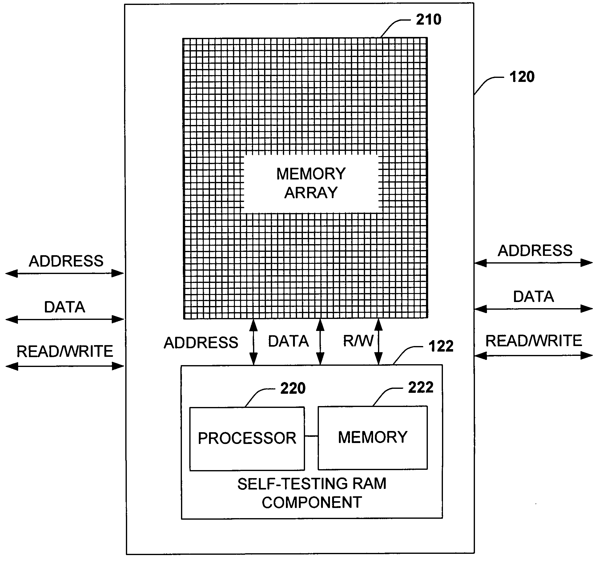
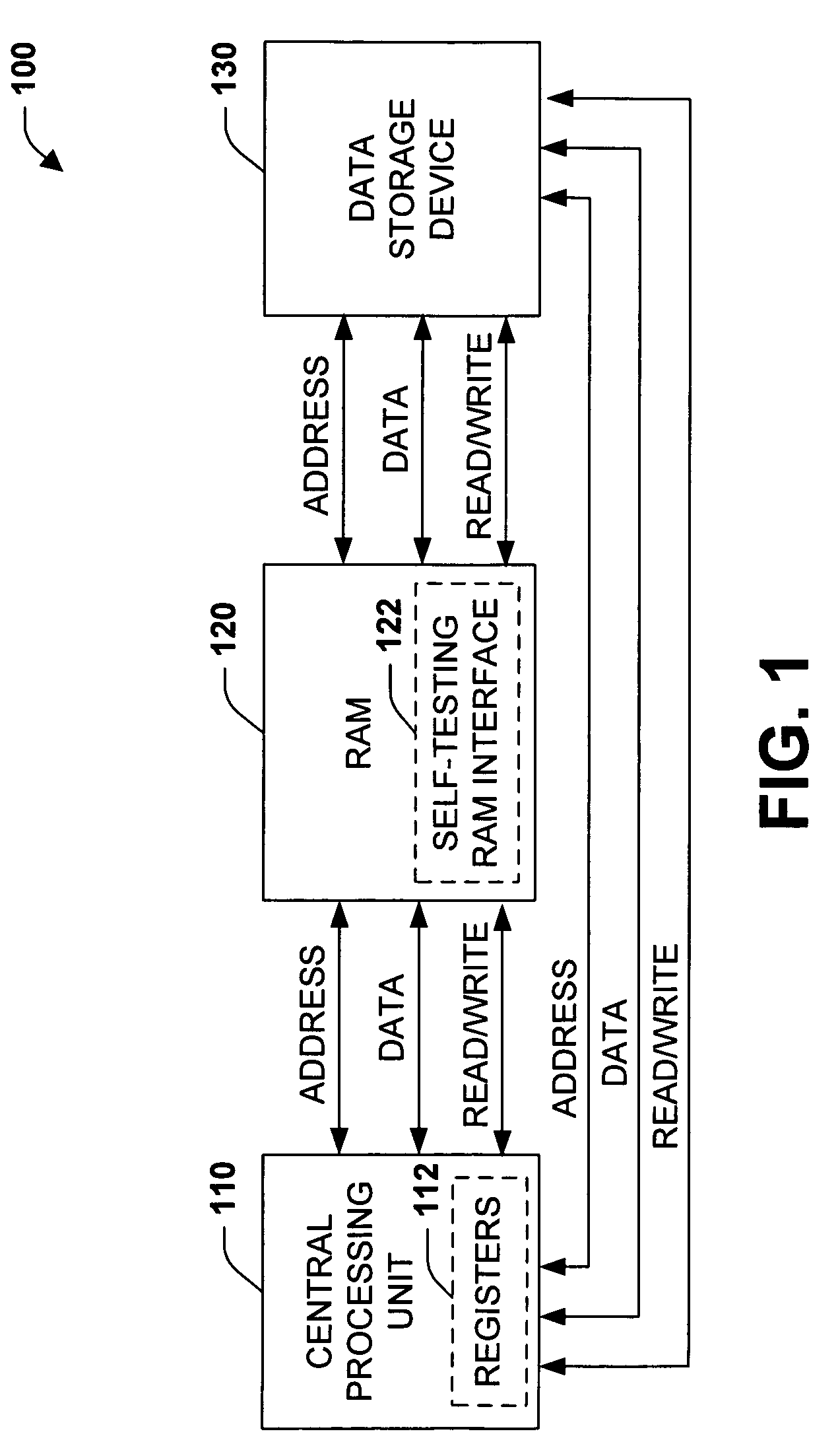
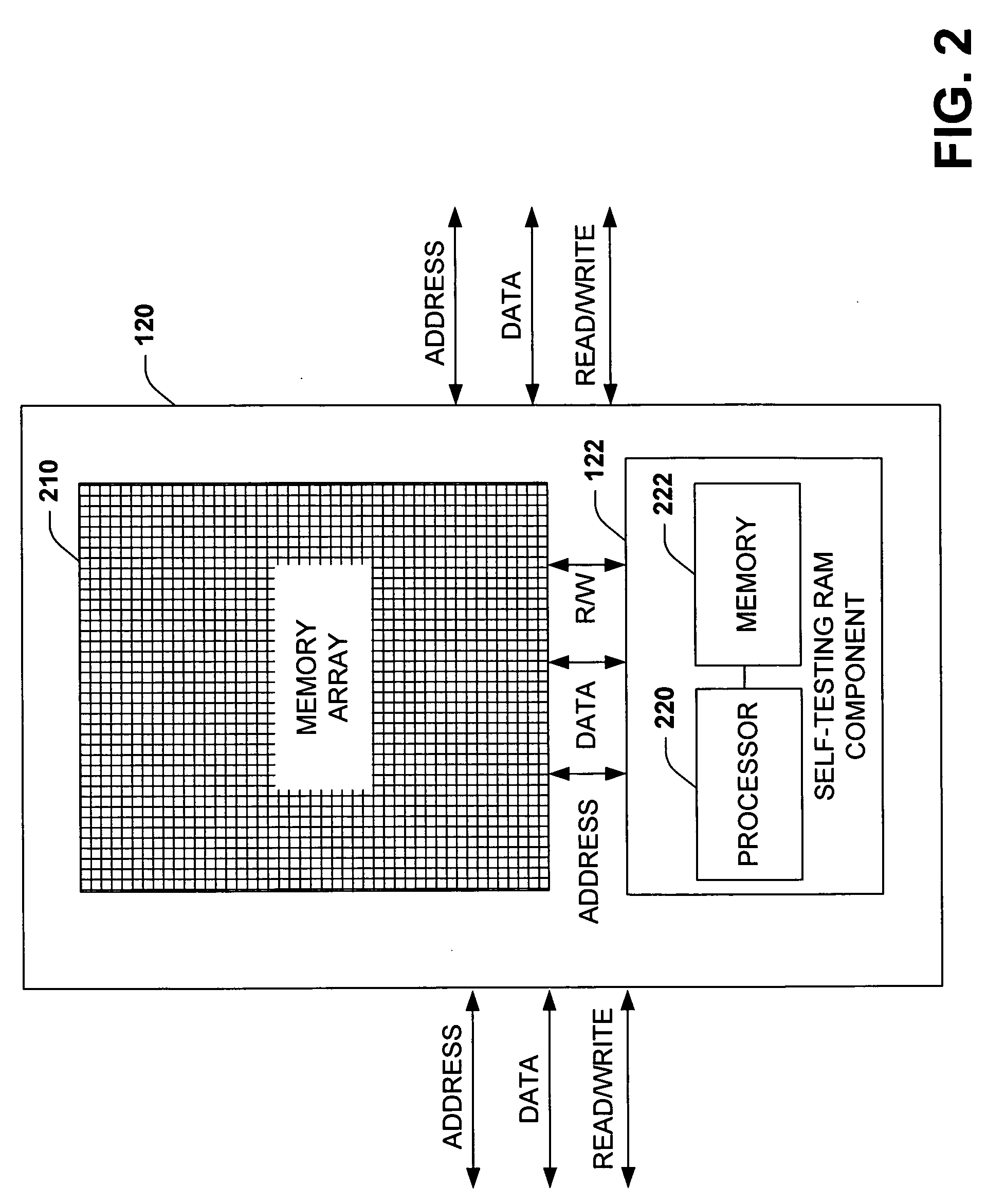
[0011] In accordance with one aspect of the present invention, a random access memory (RAM) device, which can self-test and self-correct memory errors, is provided. The RAM device or card contains a memory array and an embedded self-testing RAM interface (also referred to herein as simply RAM interface or interface), which contains appropriate logic or a microprocessor that facilitates, among other things, testing of the memory array. The unique architecture of the present invention frees a central processing unit (CPU) from having to execute tedious memory testing algorithms on a large amount of data. According to one aspect of the invention, the self-testing RAM can execute all the tests that would conventionally need CPU intervention. According to another aspect of the invention, the CPU and the self-testing RAM interface can cooperate and testing duties can be divided amongst both the CPU and the self-testing RAM interface in an optimal fashion.
[0012] Testing of memory can vary in complexity depending on the nature of the test and the allotted time for test completion. As describe supra, conventionally a computer boot process is delayed in proportion to the amount of RAM on the platform. The present invention, however, can mitigate or even eliminate the conventional start up delay without having to forgo RAM testing (e.g., quick boot). By dividing testing duties between the CPU and the self-testing RAM device, start-up times can be cut in half or more. Further yet, according to another aspect of the invention, upon system start-up the self-testing RAM interface can effectuate all the testing procedures and make portions of RAM available to the CPU, concurrently running the boot process, in real-time after it is tested.
[0016] According to still another aspect of the subject invention, the RAM interface can be employed to facilitated secure storage of data to memory. In particular, a CPU interface can be utilized to retrieve and / or receive data, read / write indicators, and addresses from the central processing unit. A data storage component can then utilize information provided by the CPU interface to store and retrieve data. To store data, a data storage component can generate a location for storage that may be different from that specified by the central processing unit. Conventionally, related data is stored in contiguous memory cells, which makes it easy for an attacker to decipher the captured memory contents. Thus, in accordance with one aspect of the invention, related data can be stored in noncontiguous memory cells to increase the difficultly of discovering memory contents. For example, the data storage component can randomly generate a memory location from available memory locations to store data thereto. In this manner, related data can be scrambled amongst one or more memory arrays to make it exponentially more difficult for an unauthorized entity to comprehend. The actual location where the data is stored can be indicated by a data map that maps the CPU address to the actual memory storage address to facilitate subsequent retrieval thereof. Furthermore and in accordance with one particular aspect of the invention, the CPU and / or operating system can transmit a signature of the task or process context to the STRAM interface as a key to the process currently reading or writing to RAM such that only a process with the same context can read / write to the proper memory locations. Furthermore, data mapping algorithms, the data storage component, and / or the data map, among other components can be removable from the system, thus leaving the memory useless to attackers and rogue processes.
[0017] In accordance with another aspect of the invention, memory data can be encrypted prior to storage to provide a further layer of protection. The data can be encrypted symmetrically such that an application user can provide a key that can be used to encrypt and later decrypt stored data. According to one aspect of the invention, an encryption key (as well as other things) can be stored on a smart cart. Hence, a user can present their card to a computer system. The computer can then provide the RAM interface with the key to encrypt volatile memory data. Consequently, if a user suspended program action and removed their card, and therefore their key, the data stored in memory could not be read until the user represented the interface with their key to decrypt the stored data. It should be appreciated that the CPU may also write a signature (or key) to the self-testing RAM component, which locks read and or write access to specific memory regions in the global RAM pool. This will prevent rogue processes from reading or modifying the RAM contents while the CPU is executing other processes / tasks or access from other memory addressable bus interfaces including but not limited to VME (VersaModule Eurocard) and PCI (Peripheral Component Interconnect).
[0021] In brief, the present invention contemplates improving overall system performance by adding or associating additional processing power with otherwise passive volatile memory devices. In particular, both memory testing and data security can be performed at a lower level thereby relieving this burden at least in part from a central processor and allowing it more efficiently process trusted data.

Problems solved by technology

Moreover, the proliferation of such technology fuels a persistent demand for smaller and higher density storage devices.
Devices fabricated with sub-micron feature sizes, however, have an increased likelihood of containing errors or contaminated data.
Popular volatile memory technologies such as dynamic random access memory (DRAM) and synchronous random access memory (SRAM) are known to be susceptible to both hard errors and soft errors.
These small geometry or high-density memory cells are also more susceptible to data corruption from a variety of sources.
Hard errors or faults occur when there is a physical failure in the digital circuitry, for example due to a problem in the design or manufacturing of a device or physical deterioration.
Memory devices with hard errors experience consistently incorrect results (e.g., bit always 1 or 0).
Soft errors or transient faults occur when charged particles such as alpha particles or cosmic rays penetrate a memory cell and cause a bit(s) to flip or change states.
No matter what the type or cause, memory faults are generally unacceptable.
In certain situations, a memory error that causes a bit to change states will be almost insignificant.
For instance, if one bit in a single screen shot that appears for a spit second is off (rather than on), such an error will often go unnoticed.
However, if a single bit is flipped in a router application it may mean the difference between a message going to Boston and a message going to San Francisco.
Furthermore, small errors in military and mission critical systems could cause catastrophic damage to life and property.
However, utilizing conventional error detection and correction techniques can significantly impact system performance in part because the central processor in a computer system needs to be diverted from other processes to test and correct a memory device.
This is problematic, as more and more software applications require an increasingly large amount of RAM to store and execute programs.
In addition to errors, memory is also susceptible to security breaches.
This is problematic when memory contents include private or sensitive information (e.g., bank account number, credit card number, user name, password .
However, this method is quite costly in terms of processing time as the central processor must be diverted from other processes to overwrite values to memory.
Hence, memory is incredibly vulnerable to attack during data processing and manipulation.
In particular, it is possible that an application could tunnel through the process space into the memory and not only view the raw contents of RAM memory but also manipulate values therein to among other things control an application, produce erroneous results, and / or crash an application or the executing system.

Method used


Image

  • Self testing and securing ram system and method
  • Self testing and securing ram system and method
  • Self testing and securing ram system and method

Examples


Embodiment Construction

[0042] The present invention is now described with reference to the annexed drawings, wherein like numerals refer to like elements throughout. It should be understood, however, that the drawings and detailed description thereto are not intended to limit the invention to the particular form disclosed. Rather, the intention is to cover all modifications, equivalents, and alternatives falling within the spirit and scope of the present invention.

[0043] As used in this application, the terms “component,”“system,” and “interface” are intended to refer to a computer-related entity, either hardware, a combination of hardware and software, software, or software in execution. For example, a component may be, but is not limited to being, a process running on a processor, a processor, an object, an executable, a thread of execution, a program, and / or a computer. By way of illustration, both an application running on a server and the server can be a component. One or more components may reside ...


PUM


Abstract

A self-testing and correcting read only memory (RAM) device and methodology is disclosed herein. The device includes at least one array of memory to enable data storage and self-testing RAM interface for evaluating, correcting, and / or compensating for memory cell errors. The RAM device, via the self-testing RAM interface, supports interaction with a central processing unit (CPU) to facilitate testing of the CPU to memory interface as well as the device memory array. Furthermore, the subject invention provides for a system and method of securely storing data to volatile memory. More specifically, the RAM interface component can be employed to, among other things, store data in noncontiguous locations, encrypt / decrypt data as well as perform authentication checks to ensure the integrity of data and / or deter attacks thereon. All or significant portions of such functionality can be performed without burdening the CPU and affecting processing speed or efficiency.

Description

CROSS-REFFERENCE TO RELATED APPLICATIONS [0001] This application is a continuation-in-part of application Ser. No. 10 / 674,044, filed Sep. 29, 2003, and entitled SELF-TESTING RAM SYSTEM AND METHOD. The entirety of said application is incorporated herein by reference.TECHNICAL FIELD [0002] The present invention relates generally to computer systems, and more particularly toward random access memory and ensuring the integrity and security thereof. BACKGROUND [0003] Computer information technology continues to spread rampantly throughout our technological society. Moreover, the proliferation of such technology fuels a persistent demand for smaller and higher density storage devices. At present, computer technologies pervade many aspects of modem life in the form of portable devices such as PDA's, phones, pagers, digital cameras and voice recorders, MP3 players, and laptop computers to name but a few. Furthermore, behind the scenes, business and industry rely heavily on computers to redu...

Claims


Application Information

Patent Timeline
IPC IPC(8): G06F12/14G06F21/00G11C29/16
CPCG06F12/1408G06F21/79G11C2029/0401G11C29/16G06F21/85
Inventor CALLAGHAN, DAVID M.
Owner SITO PROCESSING
Learn More