
Semiconductor device

a technology of semiconductors and devices, applied in the field of semiconductor devices, can solve the problems of lowering the maximum operating frequency of the circuit and increasing the power dissipation, and achieve the effects of low voltage, low power dissipation, and improved circuit operation frequency

Inactive Publication Date: 2005-09-22
RENESAS ELECTRONICS CORP
View PDF4 Cites 10 Cited by
  • Summary
  • Abstract
  • Description
  • Claims
  • Application Information

AI Technical Summary

Benefits of technology

[0016] Accordingly, it is therefore an object of the present invention to provide a semiconductor circuit of a novel configuration designed to achieve the low power dissipation and a high speed operation.
[0023] According to the present invention, the operating frequency of the circuit may be improved, whilst the low voltage driving and low power dissipation may be achieved, by lowering the operating frequency of the clock line of the shift register.

Problems solved by technology

However, these requirements are in a trade-off relationship to one another.
If a signal line in need of an operating speed in excess of the targeted operation is used in a circuit intrinsically aimed to transfer the data, the result is the lowered maximum operating frequency of the circuit and the increased power dissipation.

Method used


Image

  • Semiconductor device
  • Semiconductor device
  • Semiconductor device

Examples


embodiments

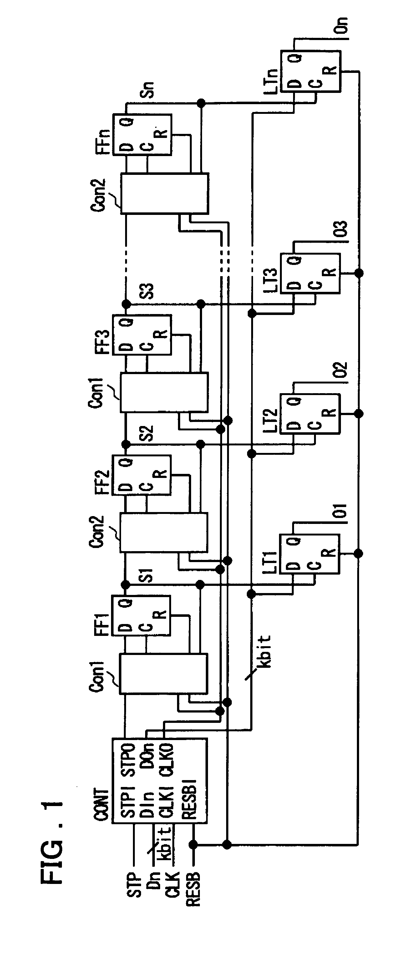
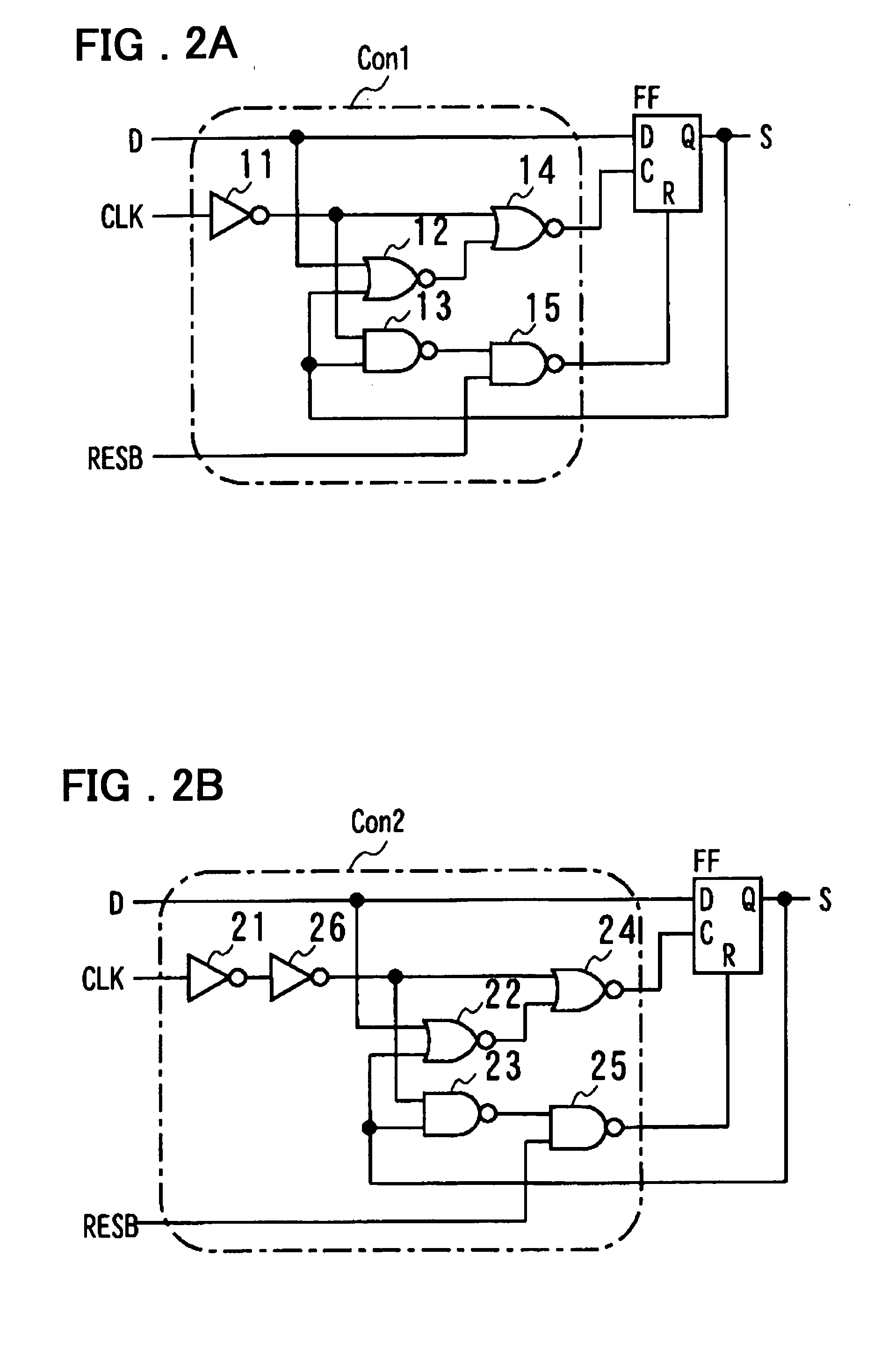
[0039]FIGS. 2A and 2B illustrate the circuit configuration of the first control circuit Con1 and the second control circuit Con2 of FIG. 1, respectively. First, the first control circuit Con1 is explained. Referring to FIG. 2A, the first control circuit Con1 includes an inverter 11 for inverting the clock signal entered to the clock input terminal CLK, a NOR circuit 12, supplied with a signal from a data input terminal D and with an output signal of the output terminal Q of the D flip-flop FF, and a NAND circuit 13, supplied with an output signal of the inverter 11 and an output signal of the output terminal Q of the D flip-flop. The first control circuit Con1 also includes a NOR circuit 14, supplied with an output signal of the inverter 11 and with an output signal of the NOR circuit 12, and a NAND circuit 15, supplied with an output signal of the NAND circuit 13 and a reset signal RESB. The signal from the data input terminal D is entered to the data input terminal D of the D flip...


PUM


Abstract

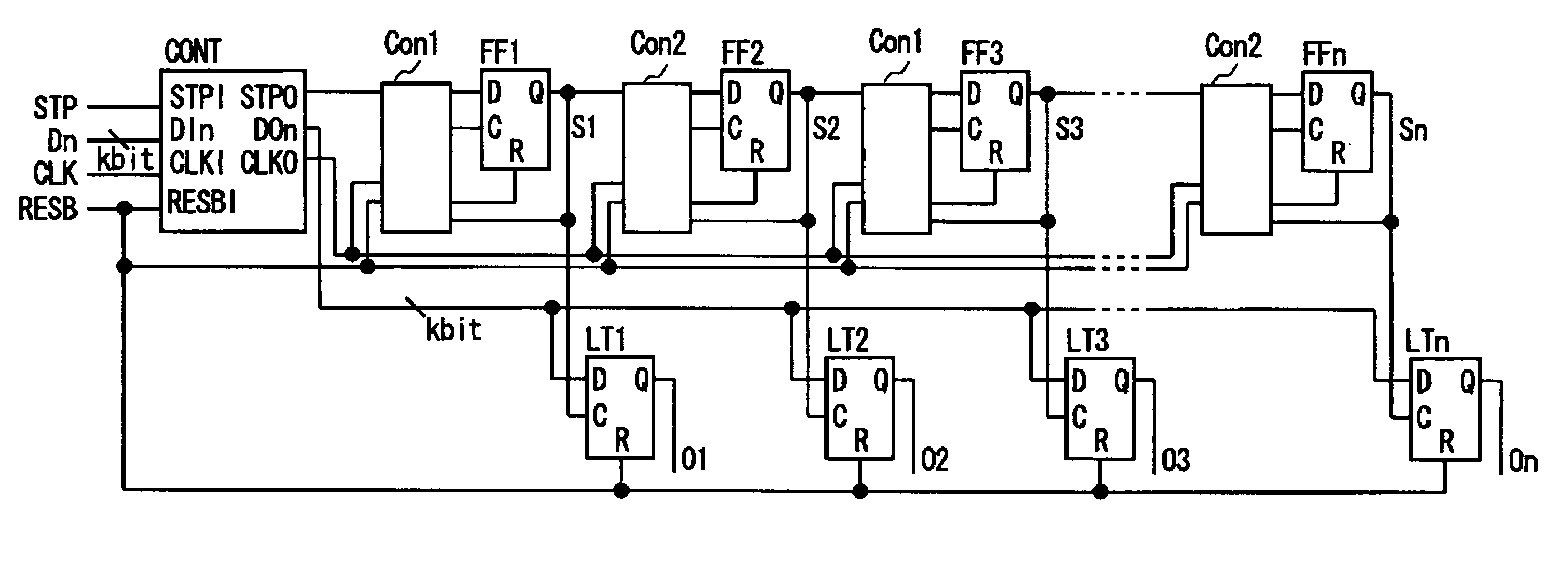
Disclosed is a serial to parallel conversion circuit in which the shift clock frequency is lowered to close to the frequency on the data line to achieve low power dissipation. The serial to parallel conversion circuit at least includes a shift register (FF1 to FFn), to the first stage of which is entered a data transfer start signal STPO and which sequentially transfers the data transfer start signal by input shift clock signal, a plural number of latch circuits (LT1 to LTn) receiving signals sequentially output from the shift register as latch clock signal to latch a data signal serially supplied to a data line, and control circuits (Con1 and Con2) receiving at least shift clock signal CLKO supplied to flip-flops and the output signals of the flip-flops. If, in case the output signals of the flip-flops are in active states, the shift clock signal supplied to the flip-flops undertakes a transition to an inactive state, the control circuits reset the flip-flops to inactivate the output signals of the flip-flops. The neighboring ones of the flip-flops sample and output signals entered to the data terminals, using one and the other of the rising and falling edges of the shift clock signal supplied from the clock line. The shift clock signal is operated at a frequency equal to one-half the data signal transfer frequency.

Description

FIELD OF THE INVENTION [0001] This invention relates to a semiconductor device and, more particularly, to a serial to parallel conversion circuit. BACKGROUND OF THE INVENTION [0002] A semiconductor device is required to be driven with low voltage, low power dissipation and a high operating frequency. In particular, the semiconductor device, used for e.g. a mobile device, is required to be driven not only with low power dissipation but with a high operating speed in keeping up with increase in the amount of data to be processed. [0003] However, these requirements are in a trade-off relationship to one another. That is, in case it is attempted to decrease the power dissipation, the operating speed is lowered, whereas, in case it is attempted to improve the operating speed, the power dissipation is increased. [0004]FIG. 7 is a diagram illustrating a typical example of a conventional serial to parallel conversion circuit. Referring to FIG. 7, this conventional circuit is described. In t...

Claims


Application Information

Patent Timeline
IPC IPC(8): H03M9/00G11C19/00G11C19/28H03M1/22
CPCH03M9/00G11C7/10G11C7/22G11C19/00
Inventor ISHIYAMA, HIROSHI
Owner RENESAS ELECTRONICS CORP
Learn More