
Solution-based fabrication of photovoltaic cell

a technology of photovoltaic cells and solutions, applied in the field of photovoltaic cells, can solve the problems of high temperature reduction and selenization steps used in each of the solar cell fabrication processes, which are neither cost effective nor easily scaled to high-volume production, and the h/sub>2/sub>se gas used is both highly toxic and flammable, and the overall cost is serious

Inactive Publication Date: 2005-08-25
AERIS CAPITAL SUSTAINABLE IP
View PDF99 Cites 324 Cited by
  • Summary
  • Abstract
  • Description
  • Claims
  • Application Information

AI Technical Summary

Benefits of technology

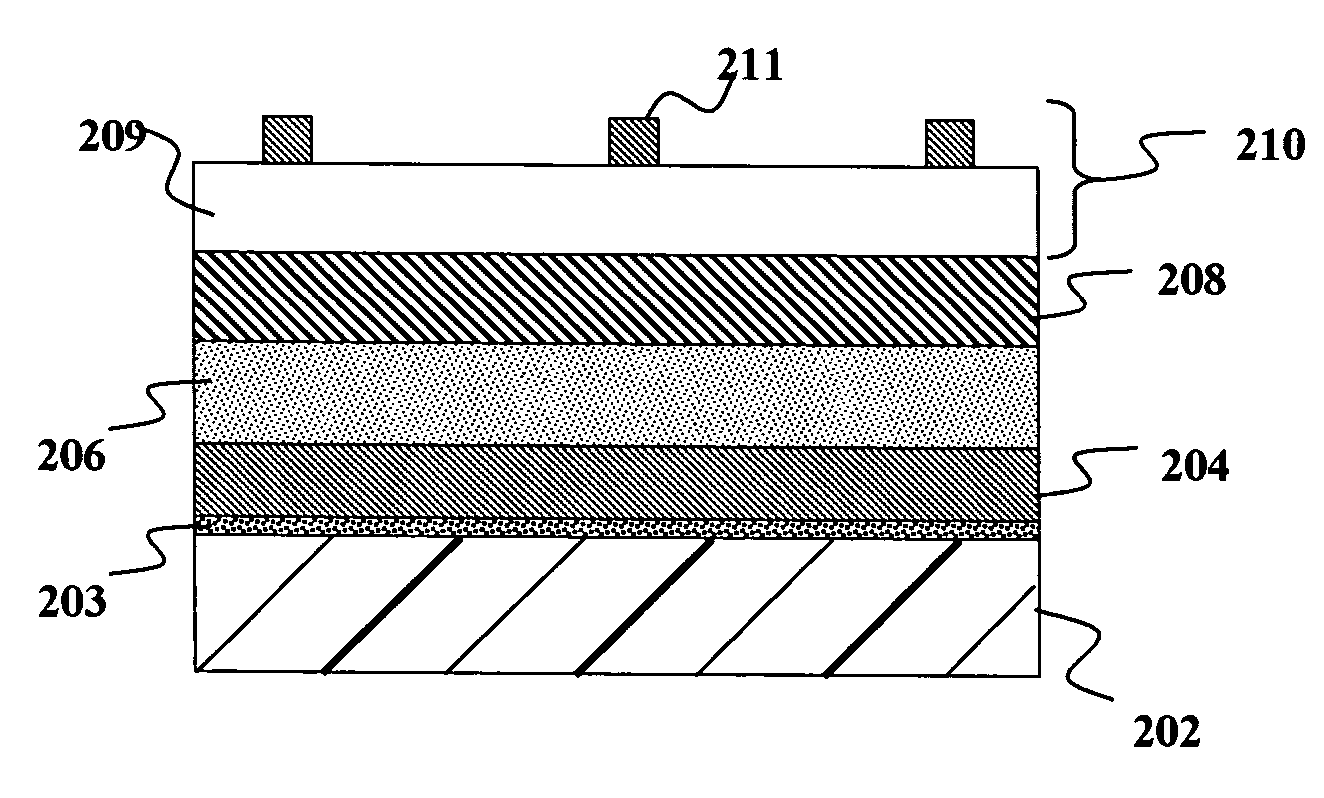
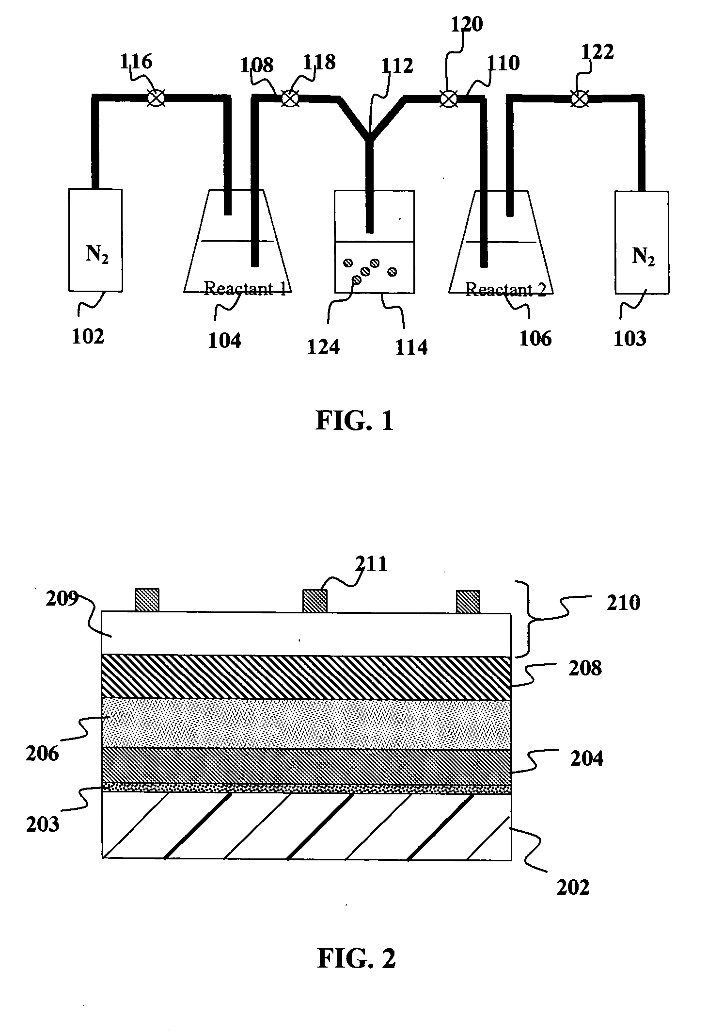
[0017] A nanoparticle-based CIGS ink has great utility for low cost web coating of ink-based photovoltaic cells. Methods to make nanoparticles of the desired materials having the desired narrow particle size distribution include controlling the reaction conditions under which the nanoparticles are made or using size-selective precipitation and other techniques (such as ultrafiltration and membrane emulsification). Nanoparticles in different categories may be incorporated into CIGS inks. These categories include but are not limited to: (1) Ternary nanoparticles such as CuInSe2 or CuInG nanoparticles; (2) Binary nanoparticles such as CuSe and In2Se3 nanoparticles; (3) Metallic nanoparticles such as Cu and In nanoparticles; (4) A suspension made using one or more liquid metals, such as Ga; (5) A liquid made using one or more organometallic precursors. Significantly, each of these approaches may be implemented without selenization of the particles, film or IB-IIIA-VIA layer using H2Se; (6) Metal halides dissolved in chelating agents; and (7) Metal salts. All of these techniques may be used to form a liquid ink. In addition, the use of non-oxide or elemental metal particles avoids having to reduce the particles, film or IB-IIIA-VIA layer with H2.

Problems solved by technology

Unfortunately, the high temperature reduction and selenization steps used in each of these solar cell fabrication processes are neither cost effective nor easily scaled to high-volume production.
Specifically, the H2Se gas used is both highly toxic and flammable.
Thus, when H2Se is used at high temperatures, safety, environmental impact, and overall cost are serious concerns in the manufacturing process.
Furthermore, the high temperature reduction and selenization steps make it impractical to make CIGS solar cells on inexpensive polymer or metallized polymer substrates that would warp, melt, or otherwise degrade at such high temperatures in the presence of reducing and / or oxidizing agents.
Although it is possible to make CIGS-based inks without using oxides, such inks have been produced in the prior art have several drawbacks for high-volume, roll-to-roll processing.
For instance, the use of bulk CuInSe2 as a starting material is challenging as bulk CuInSe2 has a melting point around 1000° C. However, since most of the flexible substrates such as Al foils and plastic foils cannot withstand such a high temperature, it is not possible to melt bulk material directly onto a substrate.
Even glass will have serious warping problems at this temperature and substrate warping typically leads to inefficient cell performance—so even with deposition onto glass, it is very difficult to create high-performance solar cells by melting bulk material.
Moreover, the energy requirements needed for high temperature manufacturing at 1000° C. will incur substantial cost.
However, annealing at a lower temperature tends to hinder the manner of crystal grain growth that is critical for the proper electronic properties of CIGS solar cell.
Unfortunately, such fluxing agents can introduce unwanted crystalline phases and alter the electronic properties of CIGS, thus lowering the efficiency of a CIGS solar cell.

Method used


Image

  • Solution-based fabrication of photovoltaic cell
  • Solution-based fabrication of photovoltaic cell

Examples


Embodiment Construction

[0009] Although the following detailed description contains many specific details for the purposes of illustration, anyone of ordinary skill in the art will appreciate that many variations and alterations to the following details are within the scope of the invention. Accordingly, the exemplary embodiments of the invention described below are set forth without any loss of generality to, and without imposing limitations upon, the claimed invention.

[0010] As used herein, the following terms have the following meanings:

“Elemental” refers to a material in substantially pure form as opposed to combined with other elements as in an alloy or in a chemical compound.

“Non-oxide” refers to a chemical moiety substantially devoid of oxygen.

[0011] Embodiments of the present invention provide several key features of a liquid ink that impact cell structure and function. The liquid ink includes particles containing elements of groups IB, IIIA and (optionally) VIA, e.g., copper and indium (with o...


PUM

PropertyMeasurementUnit
particle sizeaaaaaaaaaa
diameteraaaaaaaaaa

Abstract

An ink for forming CIGS photovoltaic cell active layers is disclosed along with methods for making the ink, methods for making the active layers and a solar cell made with the active layer. The ink contains a mixture of nanoparticles of elements of groups IB, IIIA and (optionally) VIA. The particles are in a desired particle size range of between about 1 nm and about 500 nm in diameter, where a majority of the mass of the particles comprises particles ranging in size from no more than about 40% above or below an average particle size or, if the average particle size is less than about 5 nanometers, from no more than about 2 nanometers above or below the average particle size. The use of such ink avoids the need to expose the material to an H2Se gas during the construction of a photovoltaic cell and allows more uniform melting during film annealing, more uniform intermixing of nanoparticles, and allows higher quality absorber films to be formed.

Description

CROSS-REFERENCE TO RELATED APPLICATION [0001] This application is related to commonly-assigned co-pending application Ser. No.______, titled “HIGH THROUGHPUT SURFACE TREATMENT ON COILED FLEXIBLE SUBSTRATES” (Attorney Docket No. NSL-025), which is filed the same day as the present application, the entire disclosures of which are incorporated herein by reference.FIELD OF THE INVENTION [0002] This invention is related to photovoltaic cells and more particularly to fabrication of IB-IIIA-VIA active layers for such cells. BACKGROUND OF THE INVENTION [0003] Low-cost production of solar cells on flexible substrates using printing or web coating technologies is promising highly cost-efficient alternative to traditional silicon-based solar cells. Recently, solution-based solar cells fabricated from alloys of copper (Cu) and indium (In) with selenium (Se) or sulfur (S) have been developed. Such CIGS solar cells have been fabricated using a non-vacuum process in which a water-based precursor i...

Claims


Application Information

Patent Timeline
Patent Type & Authority Applications(United States)
IPC IPC(8): A61K9/16A61K9/50B82B3/00H01L21/00H01L31/00H01L31/0256H01L31/0392H01L31/18
CPCB82Y5/00B82Y10/00B82Y30/00C23C18/1204C23C18/1266Y02E10/541H01L31/0322H01L31/06H01L31/0749H01L31/18C23C18/1295Y02P70/50
Inventor YU, DONGFIDANZA, JACQUELINEROSCHEISEN, MARTIN R.SAGER, BRIAN M.
Owner AERIS CAPITAL SUSTAINABLE IP
Learn More