
Lighting system with high and improved extraction efficiency

Inactive Publication Date: 2005-08-11
DICON FIBEROPTICS
View PDF19 Cites 91 Cited by
  • Summary
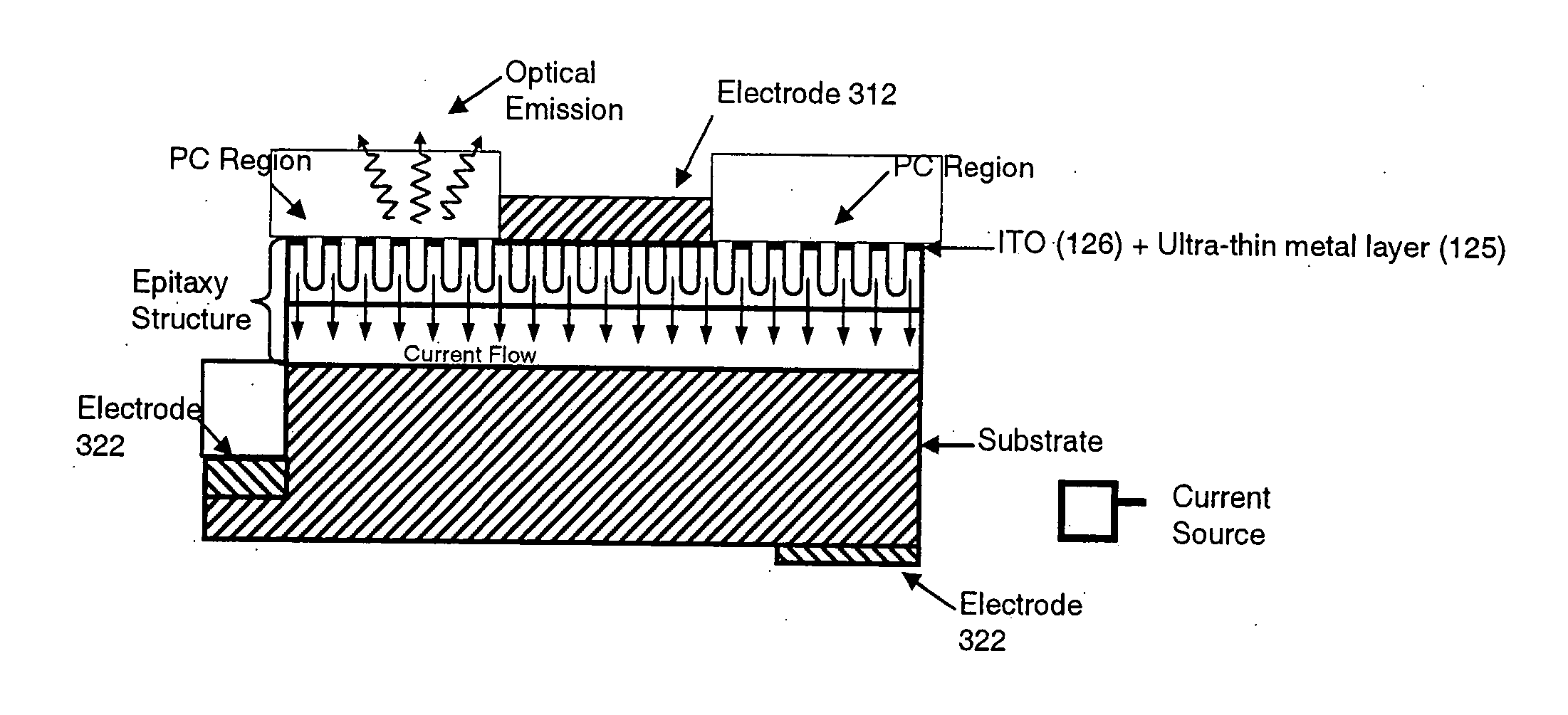
  • Abstract
  • Description
  • Claims
  • Application Information

AI Technical Summary

Benefits of technology

[0005] The present invention proposes a novel configuration for the solid state lighting systems to achieve extraction efficiency and optical emission from electrical pumping in the active layer superior to the above-mentioned conventional methods.
[0006] In an epitaxial structure of a solid state Light Emitting system, electrical current injection into the active layer is used to excite the photon emission. The invention of the parent application employs one or more structures (such as layers) different from the active layer for trapping the light generated by the active layer. Then another structure is used for extracting the light trapped. In one embodiment, the light generated by the active layer is trapped by means of a unique waveguide layer in the epitaxial structure to achieve high performance. The waveguide layer preferably traps a significant portion of the radiation generated by the active layer in a single mode (e.g. its fundamental mode) or a few lower-order modes. This feature of the parent application is a completely new feature in solid state lighting system design. Furthermore, one embodiment of the parent application employs multiple photonic crystal regions located either outside or inside one or more current injection regions to extract photons from the waveguide layer(s). This novel design optimizes the interplay of electrical pumping, radiation and optical extraction to increase the optical output to several times that of conventional solid state lighting systems. In another embodiment of the parent application, a transparent and conductive ITO layer is added to the surface of an epitaxial structure to reduce the interface reflection in addition to functioning as a current spreading layer. Each of the above-described features can be used separately or in conjunction with any one of the other features for improved performance. The invention of the parent application creates solid state lighting systems with high optical output and high power efficiency.

Problems solved by technology

This is a challenging problem because the chip may have a much higher index of refraction, typically 3.4 for GaAs-based material, compared with 1.0 for air and approximately 1.5 for epoxy.
None of these approaches is entirely satisfactory.

Method used


Image

  • Lighting system with high and improved extraction efficiency
  • Lighting system with high and improved extraction efficiency
  • Lighting system with high and improved extraction efficiency

Examples


Embodiment Construction

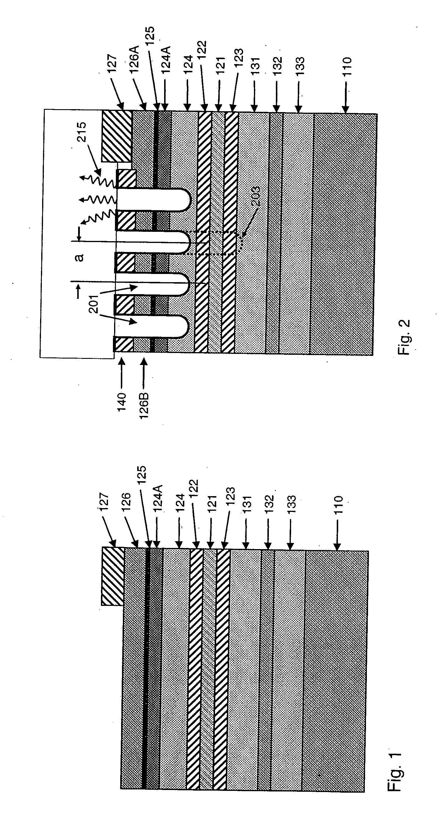
[0026] In order to illustrate one embodiment of the invention of the parent application directed to a solid state lighting system having a photonic crystal (PC) structure with clarity, we first present an epitaxial structure suitable for implementing photonic crystal and then add the photonic crystal structure into the epitaxial structure. FIG. 1 shows the epitaxial structure of the present invention without the PC structure. All epitaxial layers are grown on the top of the substrate 110. The substrate material is typically GaAs for red or yellow light emission structures and Sapphire, GaN or SiC for UV, blue and green light emission structures. Layer 121 is the active layer, where holes and electrons combine to emit light. The epitaxial structure of active layer 121 can be double heterostructure, multi-quantum wells (MQWs), or multi-quantum dots (MQDs) to optimize the internal quantum efficiency.

[0027] Holes and electrons combine in the active layer 121, causing light to be sponta...


PUM


Abstract

In an epitaxial structure of a solid state lighting system, electrical current injection into the active layer is used to excite the photon emission. The present invention employs a unique waveguide layer in the epitaxial structure for trapping the light generated by the active layer in the fundamental waveguide mode. Multiple photonic crystal regions with different characteristics located either outside or inside one or more current injection regions extract photons from the waveguide layer(s). The present invention creates solid state lighting with high optical output and high power efficiency.

Description

CROSS-REFERENCE TO RELATED APPLICATION: [0001] This application is a continuation-in-part application of U.S. patent application Ser. No. 10 / 773,943 filed Feb. 6, 2004, entitled “SOLID STATE LIGHTING SYSTEM WITH HIGH EXTRACTION EFFICIENCY” by Ho-Shang Lee and Alexander Birman, herein referred to as the “Parent Application”. The Parent Application is herein incorporated herein by reference in its entirely.BACKGROUND OF THE INVENTION [0002] Rapid advances in solid state lighting systems such as high-brightness Light emitting diode (HB-LED) technology in the last decade have opened up the possibility of using LEDs as sources of general illumination in the not-too-distant future. Remarkable progress in LED efficiency, lifetime and total lumen output has enabled an early market in niche lighting applications such as traffic lights, brake lights, mobile phones, and outdoor signs. The rapid progress in LED technology has led to the belief that LED could have a significant impact on the lig...

Claims


Application Information

Patent Timeline
IPC IPC(8): H01L21/00H01L33/08H01L33/24
CPCH01L33/08H01L2933/0083H01L33/24
Inventor LEE, HO-SHANGBIRMAN, ALEXANDER
Owner DICON FIBEROPTICS
Learn More