Digital filter design method and device, digital filter design program, and digital filter
a filter and design method technology, applied in the field of digital filter design methods and devices, digital filter design programs and digital filters, can solve the problems of difficult to set window functions or approximate expressions appropriately, not being able to easily design filters with desired characteristics, and not being able to obtain satisfactory frequency characteristics, etc., to prevent the generation of discretization errors in the filter coefficient obtained, reduce the number of circuit elements, and eliminate the use of window functions
- Summary
- Abstract
- Description
- Claims
- Application Information
AI Technical Summary
Benefits of technology
Problems solved by technology
Method used
Image
Examples
first embodiment
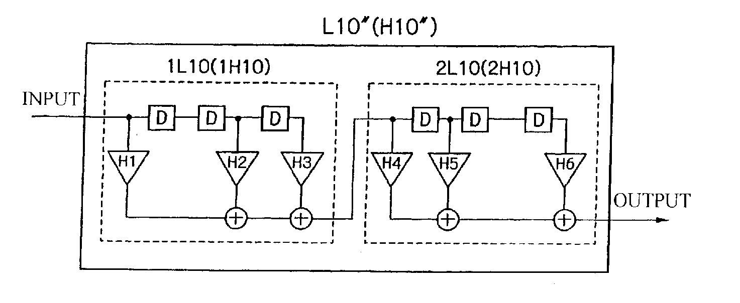
[0044] The filter design method according to a first embodiment is designed to create unit filters L1n″, H1n″ (basic filters of the present invention) which will be described below, and allow an FIR filter having a desired frequency characteristic to be designed using only one of them. The suffix “n” to each numeral indicating the unit filter denotes the number of clocks of a delay to be inserted between taps, that is, the number of “0”s to be inserted between filter coefficients (which will be explained in detail later).
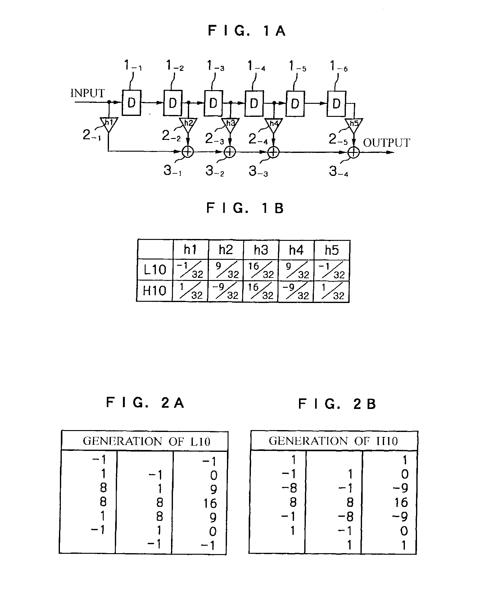
[0045] First, two types of 5-tap unit filters L1n, H1n which serve as a reference in understanding the above described unit filters L1n″, H1n″ will be explained. FIGS. 1A and 1B are diagrams showing the 5-tap unit filters L10, H10. FIG. 1A shows the circuit structure and FIG. 1B shows numerical sequences of filter coefficients.
[0046] As shown in FIG. 1A, the 5-tap unit filters L10, H10 delay an input signal sequentially by 1 clock CK at a time using six cascade co...
second embodiment
[0130] Next, a second embodiment of the present invention will be described. FIGS. 22A and 22B are diagrams showing the above described low-pass filter {1L(2.6)10*2L(2.6)10}64, FIG. 22A shows the circuit structure and FIG. 22B shows clocks to be used.
[0131] The low-pass filter shown in FIG. 22 is constructed of D-type flip flops 51, 56 operating on a reference clock CK, D-type flip flops 53 and 4-stage processing section 54 operating on a 16 times frequency clock 16CK, and a multiplexer 52 and data selector 55 operating on a 1 / 16 times frequency clock CK1. The 4-stage processing section 54 is constructed of a low-pass filter {1L(2.6)116*2L(2.6)116}4.
[0132] The data input to the D-type flip flop 51 which is the first stage is input to the terminal A side of the multiplexer 52. Data which is the result of low-pass filter processing output from the terminal B of the data selector 55 is input to the terminal B side of this multiplexer 52. The multiplexer 52 selectively outputs any one...
PUM
 Abstract
Description
Claims
Application Information
 - R&D
- Intellectual Property
- Life Sciences
- Materials
- Tech Scout
- Unparalleled Data Quality
- Higher Quality Content
- 60% Fewer Hallucinations
Browse by: Latest US Patents, China's latest patents, Technical Efficacy Thesaurus, Application Domain, Technology Topic, Popular Technical Reports.
© 2025 PatSnap. All rights reserved.Legal|Privacy policy|Modern Slavery Act Transparency Statement|Sitemap|About US| Contact US: help@patsnap.com


