Spatial light modulator and method for performing dynamic photolithography

Inactive Publication Date: 2005-06-16
AGILENT TECH INC
View PDF10 Cites 10 Cited by
  • Summary
  • Abstract
  • Description
  • Claims
  • Application Information

AI Technical Summary

Benefits of technology

[0012] By shifting data through the memory elements of the spatial light modulator in the photolithography system, the amount of data loaded into the spatial light modulator for each image transfer is reduced, thereby increasing throughput rates. In addition, because the memory of the spatial light modulator can be configured to move the data bi-directionally, the substrate can be translated bi-directionally, which can further increase throughput rates.

Problems solved by technology

Although the use of a mask provides for a high degree of precision and repeatability, traditional contact photolithography systems suffer from several limitations.
One limitation is a manufacturing specification that restricts the size of the substrate to no greater than the size of the mask.
For large substrates, it is difficult to produce and handle a mask of sufficient size to cover the entire substrate area.
Large masks are both unwieldy and expensive to produce.
However, the cost to design and embed a pattern on a mask is considerable, and therefore, creating a large number of masks may be cost-prohibitive.
Likewise, in applications where frequent changes occur, creating a new mask each time a change occurs may not be cost effective.
As a result of the multiple imaging process, each defective light modulation element will produce numerous defects on the substrate surface.

Method used


Image

  • Spatial light modulator and method for performing dynamic photolithography
  • Spatial light modulator and method for performing dynamic photolithography
  • Spatial light modulator and method for performing dynamic photolithography

Examples


Embodiment Construction

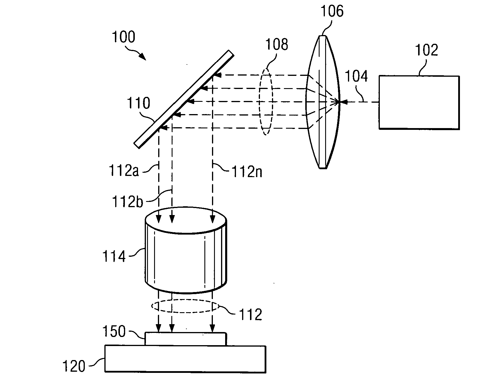
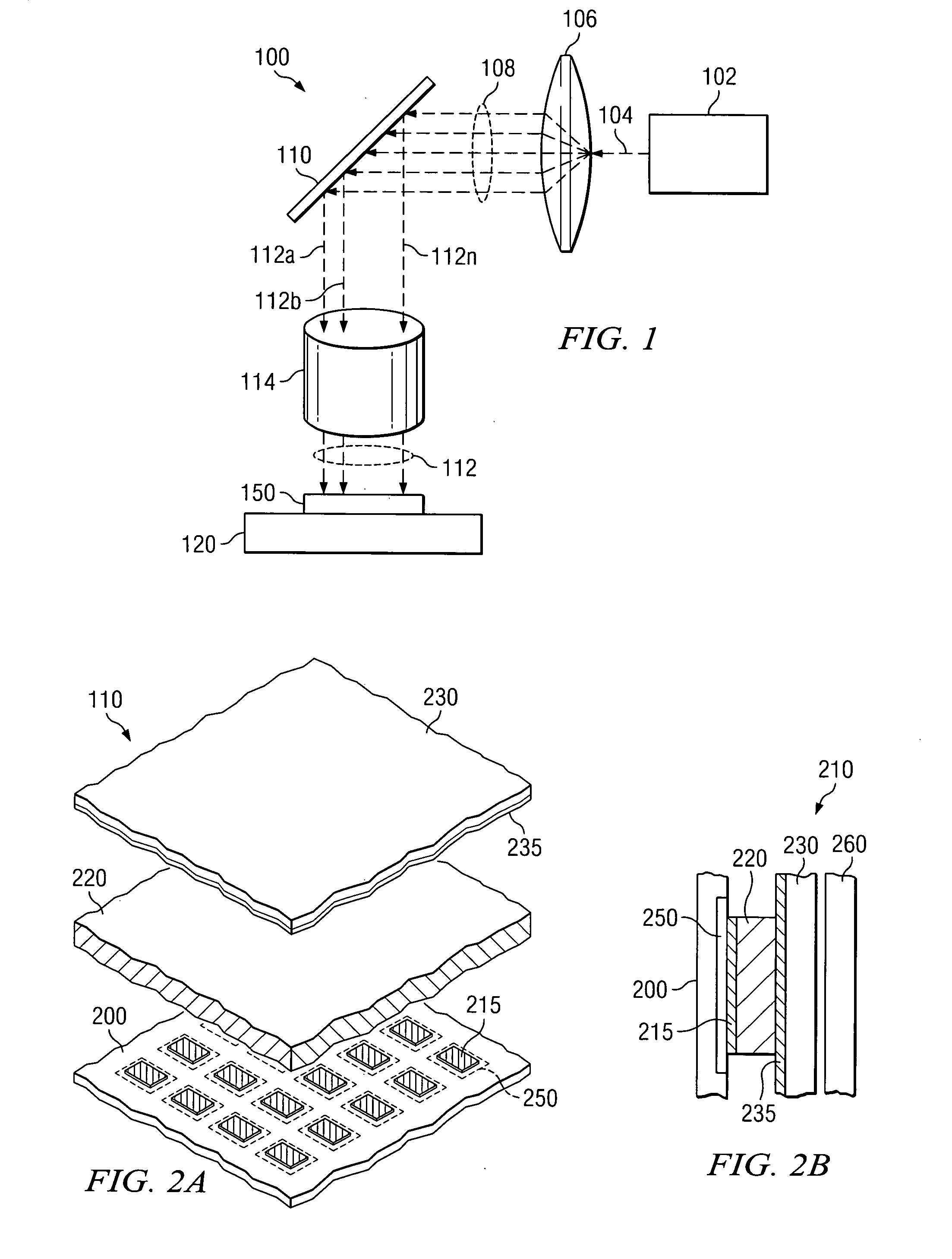
[0033]FIG. 1 illustrates a dynamic photolithography system 100 for photolithographically transferring an image to a substrate 150 in accordance with embodiments of the present invention. The photolithography system 100 includes a light source 102 operable to output light 104. The light source 102 can be a laser, such as an excimer laser, or other non-laser source, as understood in the art. The light source 102 is optically coupled to beam shaping optics 106. The output of the beam shaping optics 106 is light 108 that is directed toward a spatial light modulator 110. The spatial light modulator 110 includes light modulation elements (not shown) operable to selectively transfer the light 108. The light modulation elements are described in more detail below in connection with FIGS. 2A and 2B. In one embodiment, the light modulation elements are liquid crystal elements. However, it should be understood that in other embodiments, the light modulation elements are micromirrors or another ...


PUM


Abstract

A spatial light modulator is configured to photolithographically transfer an image onto a substrate with reduced bandwidth. The spatial light modulator includes memory elements configured to store data therein and move data therebetween. Light modulation elements are in communication with respective ones of the memory elements and are operable to be altered in response to the data stored in the respective memory elements. The memory elements can be configured as a shift register to shift the data bi-directionally between the memory elements. Each memory element can further include a feedback element, where the feedback element is a “weak” feedback element that is utilized to contribute to maintaining a voltage to minimize photocurrent effects.

Description

CROSS-REFERENCE TO RELATED APPLICATIONS [0001] This application is related by subject matter to U.S. Utility applications for Patent Attorney Docket No. 10030518, entitled REAL TIME IMAGE RESIZING FOR DYNAMIC DIGITAL PHOTOLITHOGRAPHY; Ser. No. 10031375, entitled DEFECT MITIGATION IN SPATIAL LIGHT MODULATOR USED FOR DYNAMIC PHOTOLITHOGRAPHY; and Ser. No. 10040070, entitled LIQUID CRYSTAL CELL THAT RESISTS DEGRADATION FROM EXPOSURE TO RADIATION, each filed on an even date herewith.BACKGROUND OF THE INVENTION [0002] 1. Technical Field of the Invention [0003] The present invention relates generally to photolithography, and more specifically, to dynamic photolithography systems. [0004] 2. Description of Related Art [0005] Photolithography is a method of transferring a pattern or image onto a substrate. Some industrial uses of photolithography include the manufacture of products, such as flat panel displays, integrated circuits (ICs), IC packaging, planar lightwave circuits (photonics), p...

Claims


Application Information

Patent Timeline
IPC IPC(8): G02BG02F1/03G02F1/07G03F7/20
CPCG03F7/70508G03F7/70291G02B26/02G02B26/08G02F1/00
Inventor NISHIMURA, KEN A.SCHROEDER, DALE W.
Owner AGILENT TECH INC
Why Eureka
Try Eureka