Composition for forming organic insulating film and organic insulating film formed from the same
a technology of organic insulating film and organic insulating film, which is applied in the direction of thermoelectric device junction material, solid-state device, electrical apparatus, etc., can solve the problems of inability to replace inorganic insulating film, inability to meet the requirements of plastic substrates, and inability to meet the requirements of organic solvents, etc., to achieve excellent chemical resistance to organic solvents and improve the electrical performance of transistors
- Summary
- Abstract
- Description
- Claims
- Application Information
AI Technical Summary
Benefits of technology
Problems solved by technology
Method used
Image
Examples
example 2
PREPARATIVE EXAMPLE 2
Preparation of Coating Solution for Formation of Organic Insulating Film
[0073] 7 g of the organic insulating polymer prepared in Preparative Example 1, 1.5 g of poly(ethylene-co-methyl acrylate-co-glycidyl methacrylate) of Formula 21a below (Aldrich) as a crosslinking agent, 1.5 g of poly(ethylene-co-methyl acrylic acid) of Formula 21b below (Aldrich) as another crosslinking agent, and 0.1 g of a photoacid generator of Formula 22 below (PAC200, Miwon Commercial Co. Ltd., Korea) were dissolved in a mixed solution of 73 g of cyclohexanone and 4.5 g of diethylene glycol methyl ethyl ether to prepare a coating solution for the formation of an organic insulating film.
example 1
Fabrication of Organic Thin Film Transistor
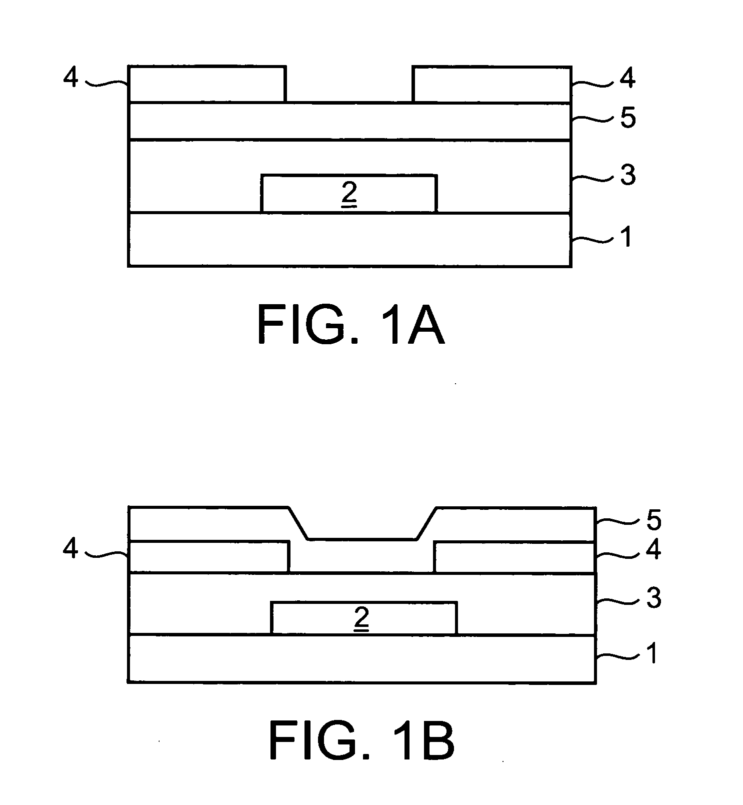
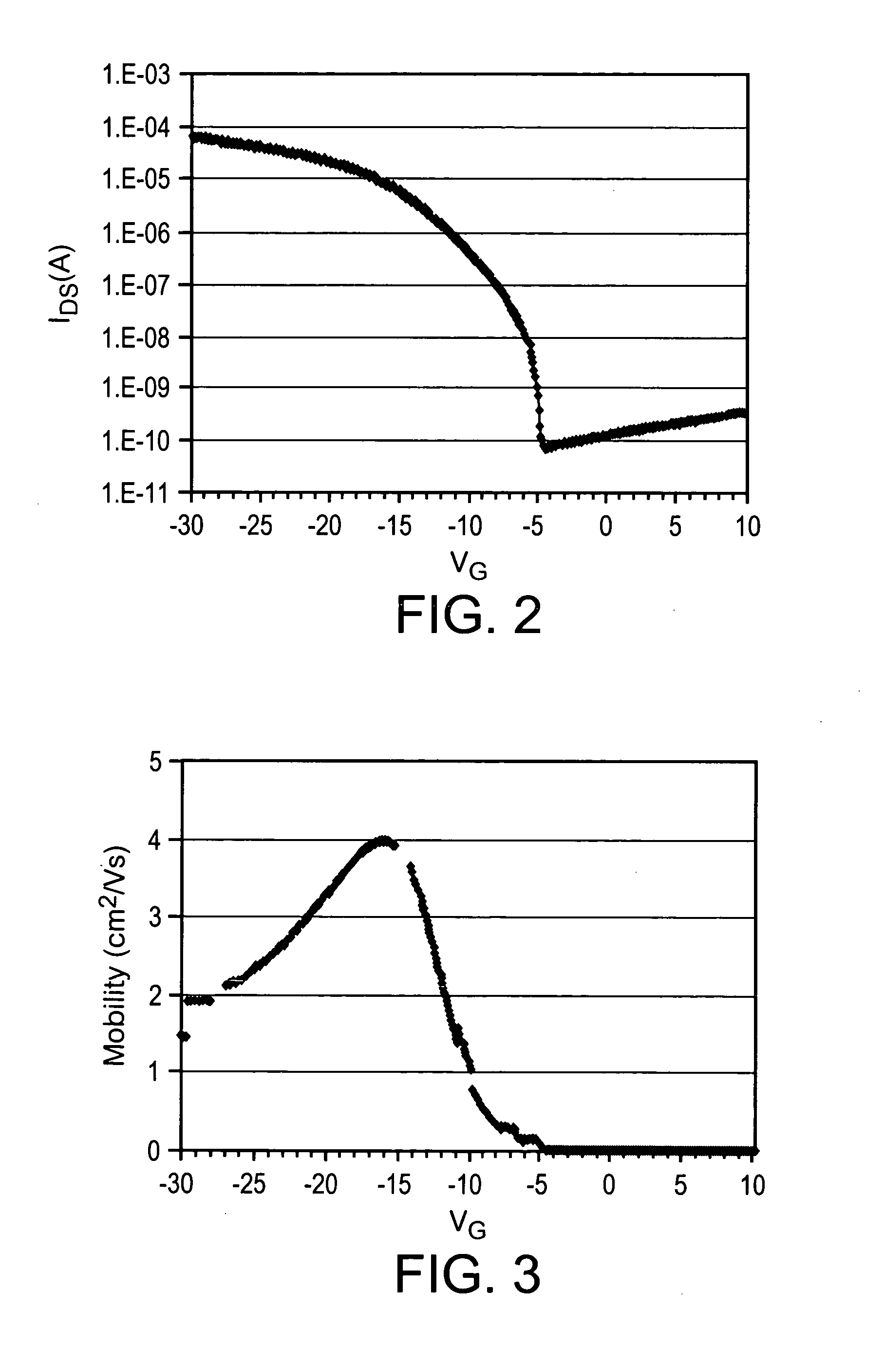
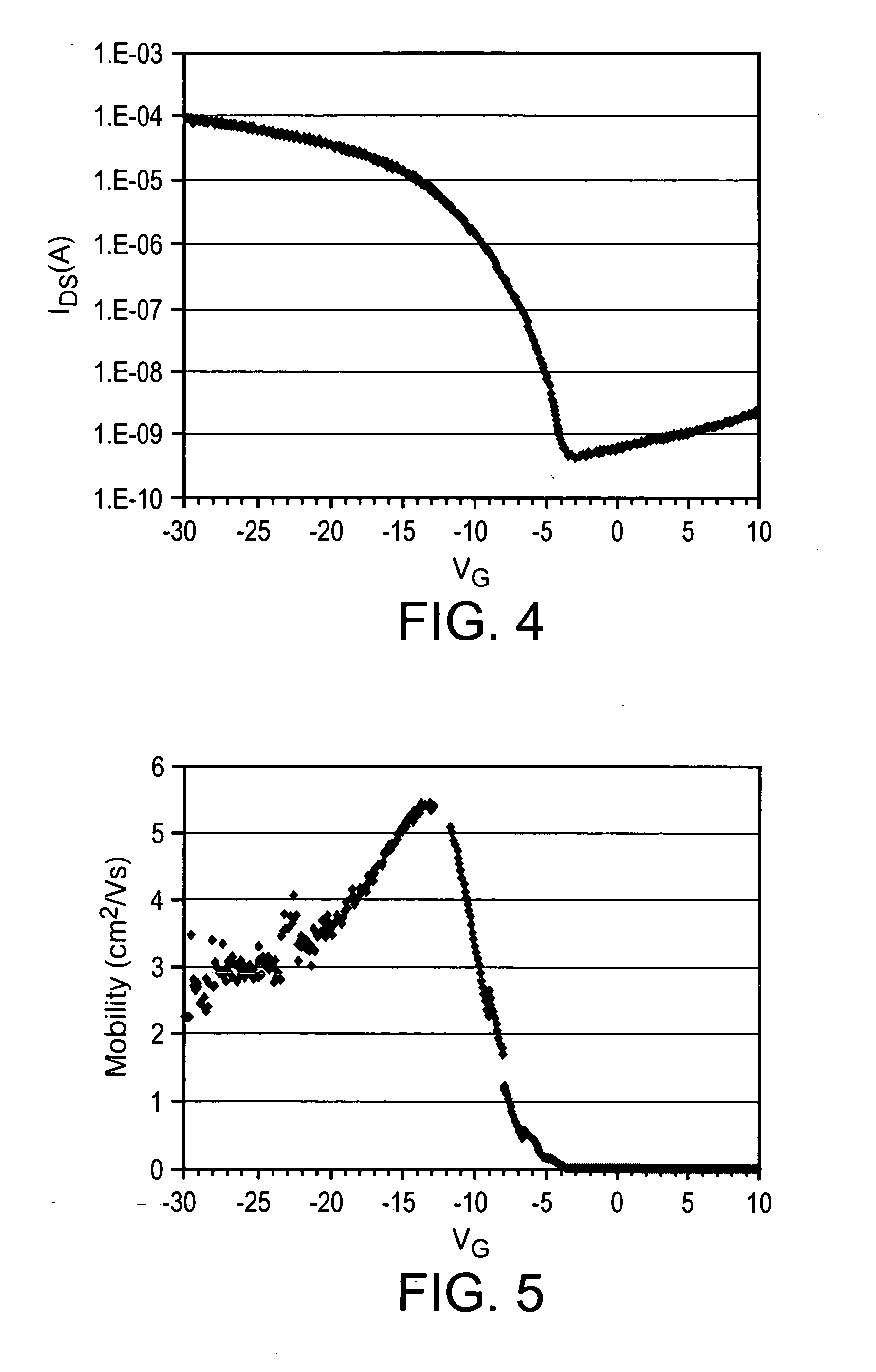
[0074] In this example, a bottom-contact organic thin film transistor was fabricated (FIG. 1b). First, Al was deposited on a washed glass as a substrate by a vacuum deposition technique to form a gate electrode having a thickness of 1,500 Å. The coating solution for forming an organic gate insulating film, which was prepared in Preparative Example 2, was coated onto the gate electrode to a thickness of 5,000 Å by spin coating at 4,000 rpm, prebaked at 100° C. for 3 minutes, irradiated by 600 W UV for 20 seconds, and baked at 100° C. for 1 hour to form an organic insulating film. Next, Au was deposited on the organic gate insulating film to a thickness of 1,000 Å, and was subjected to a photographic process to form an Au electrode pattern. Pentacene was deposited on the Au electrode pattern to a thickness of 1,000 Å by organic molecular beam deposition (OMBD) under a vacuum of 2×10⁻⁷ torr, a substrate temperature of 50° C. and a deposition ...
PUM
| Property | Measurement | Unit |
|---|---|---|
| Percent by mass | aaaaa | aaaaa |
| Percent by mass | aaaaa | aaaaa |
| Percent by mass | aaaaa | aaaaa |
Abstract
Description
Claims
Application Information
 - R&D
- Intellectual Property
- Life Sciences
- Materials
- Tech Scout
- Unparalleled Data Quality
- Higher Quality Content
- 60% Fewer Hallucinations
Browse by: Latest US Patents, China's latest patents, Technical Efficacy Thesaurus, Application Domain, Technology Topic, Popular Technical Reports.
© 2025 PatSnap. All rights reserved.Legal|Privacy policy|Modern Slavery Act Transparency Statement|Sitemap|About US| Contact US: help@patsnap.com


