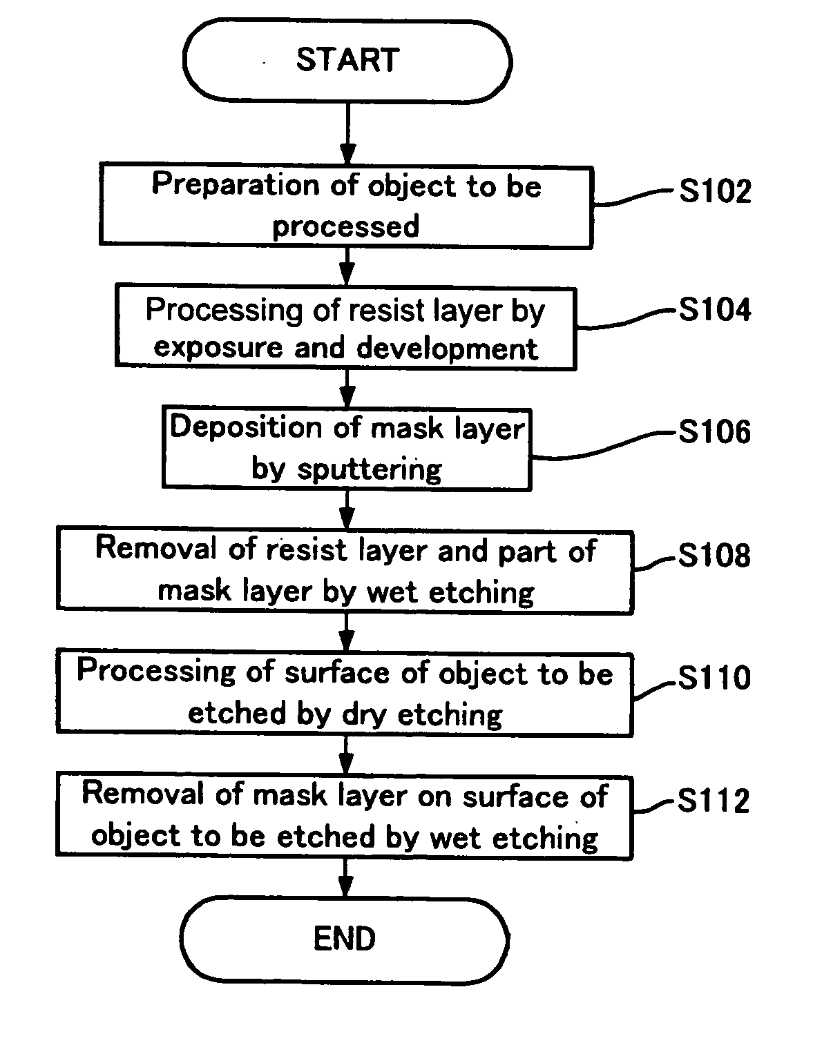
Master for concavo-convex pattern transfer and method for manufacturing stamp for manufacturing information recording medium
a technology of concave and convex patterns, applied in the direction of patterned record carriers, nanoinformatics, instruments, etc., can solve the problems of unlikely deformation or breakage of the mask, and achieve the effect of high accuracy, high accuracy and efficient manufacturing
- Summary
- Abstract
- Description
- Claims
- Application Information
AI Technical Summary
Benefits of technology
Problems solved by technology
Method used
Image
Examples
working example 1
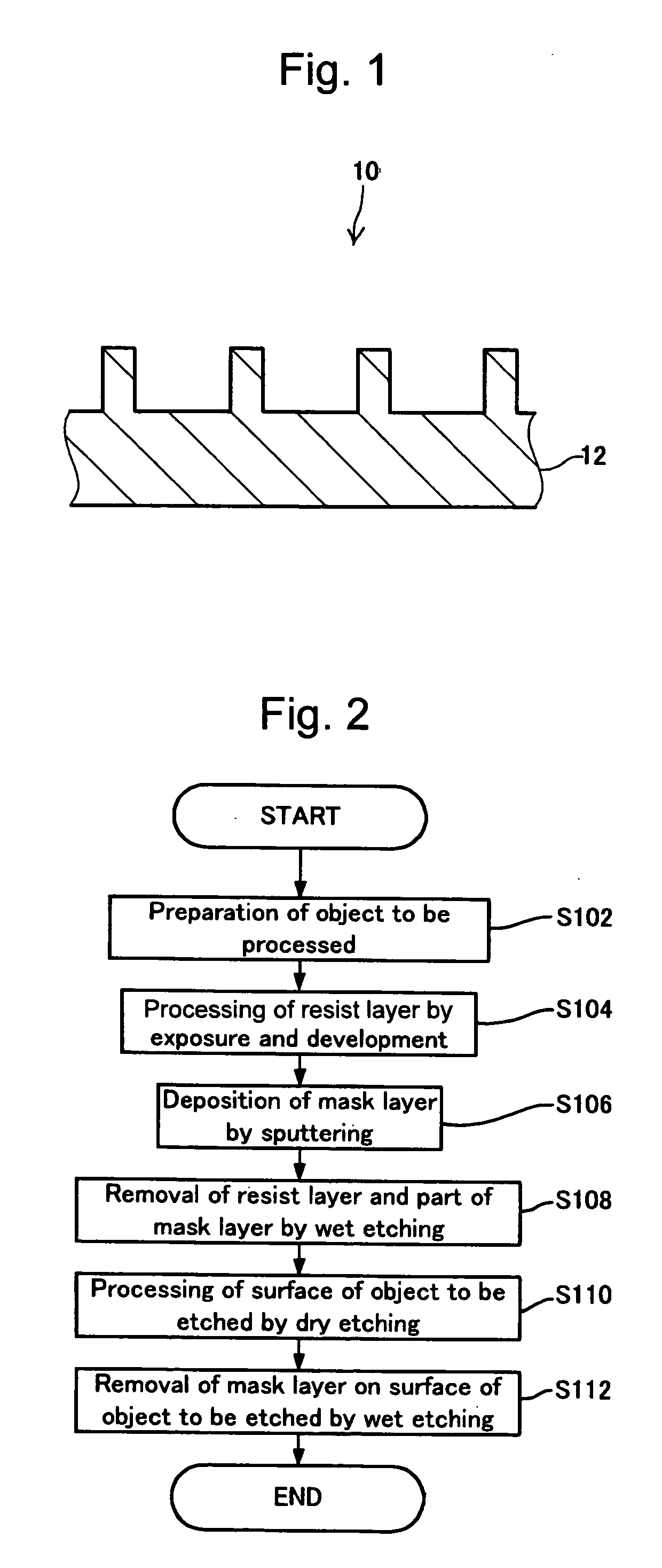
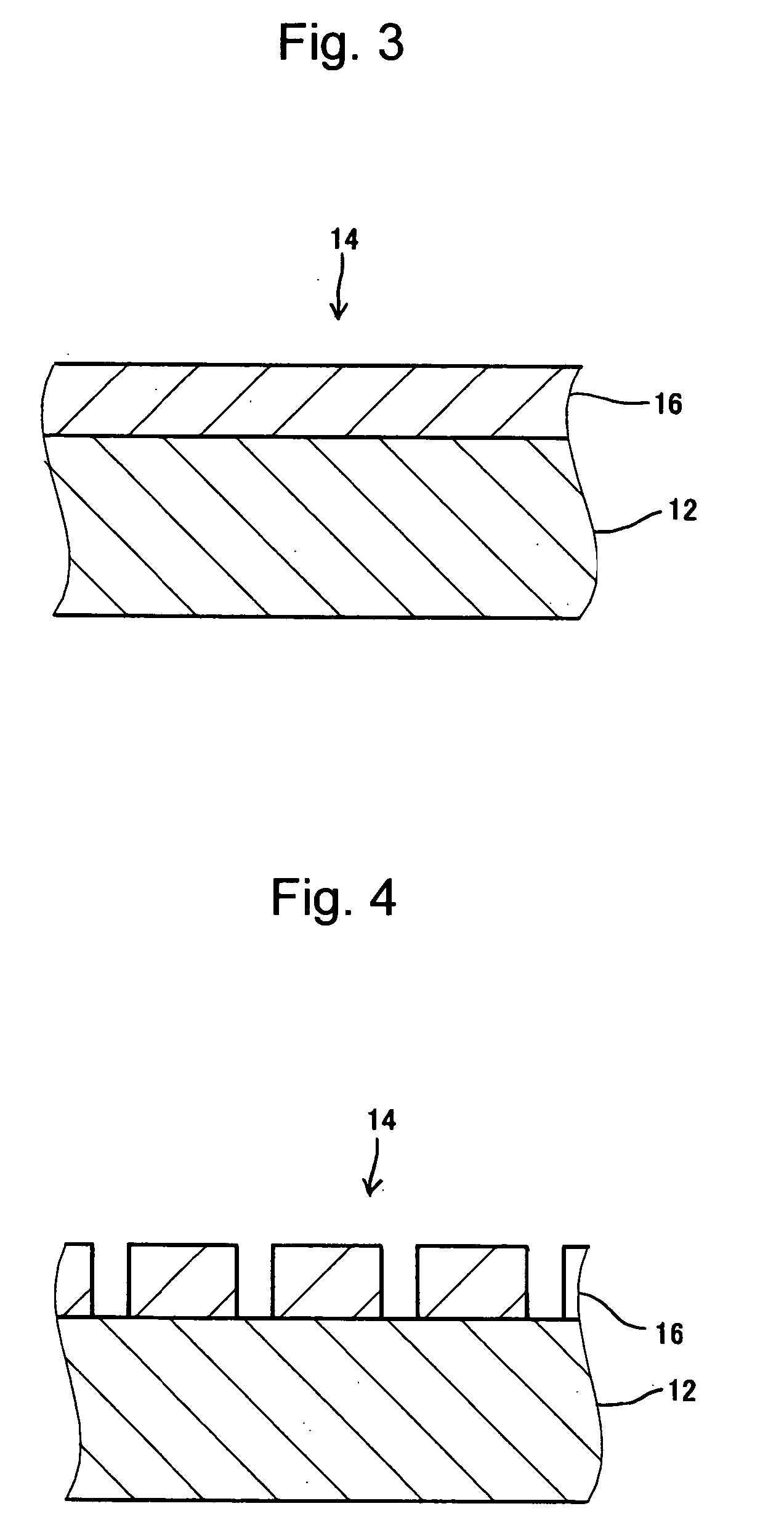
[0073] In the manner as described in the first exemplary embodiment above, the master 10 for concavo-convex pattern transfer was manufactured. Specifically, the concavo-convex patterns of an object to be etched, a mask layer, and a resist layer were formed in the following size. As a material of the resist layer 16, a positive electron beam resist ZEP520A (Zeon Corporation) was used.
Object to be Etched:
[0074] Pitch of concavo-convex pattern: approx. 150 nm
[0075] Width of convex portion: approx. 50 nm
[0076] Width of concave portion: approx. 100 nm
[0077] Level difference between concavity and convexity: approx. 150 nm
Resist Layer:
[0078] Thickness: 90 nm
[0079] Width of convex portion: approx. 100 nm
[0080] Width of a concave portion: approx. 50 nm
Mask Layer:
[0081] Thickness: 15 nm
[0082] Width of convex portion: approx. 50 nm
[0083] Width of concave portion: approx. 100 nm
[0084] A value obtained by dividing 150 nm, corresponding to the level difference between concavity a...
working example 2
[0086] A plurality of materials of the object to be etched and the mask were selected. For each combination of the materials, a concave portion having a width of approx. 100 nm and a depth of approx. 150 nm was formed on the object to be etched by reactive ion etching using an SF6 gas as a reactive gas. Then, the relation between the etching rate ratio and the angle of a lateral face of the concave portion was measured. Herein, the etching rate ratio is obtained by dividing the etching rate of the object to be etched by the etching rate of the mask material. In the process of any combination of materials, a source power of the reactive ion etching was set to 1000 W and a bias power thereof was set to 150 W. On the other hand, a pressure in a vacuum chamber was regulated in accordance with a material. The results of measurement were shown in Table 2 and FIG. 15. The pressure in the vacuum chamber was also shown in Table 2. The angle of the lateral face of the concave portion was indi...
PUM
| Property | Measurement | Unit |
|---|---|---|
| Electrical conductivity | aaaaa | aaaaa |
| Width | aaaaa | aaaaa |
| Height | aaaaa | aaaaa |
Abstract
Description
Claims
Application Information
 - R&D
- Intellectual Property
- Life Sciences
- Materials
- Tech Scout
- Unparalleled Data Quality
- Higher Quality Content
- 60% Fewer Hallucinations
Browse by: Latest US Patents, China's latest patents, Technical Efficacy Thesaurus, Application Domain, Technology Topic, Popular Technical Reports.
© 2025 PatSnap. All rights reserved.Legal|Privacy policy|Modern Slavery Act Transparency Statement|Sitemap|About US| Contact US: help@patsnap.com


