
Electrically conducting organic polymer/nanoparticle composites and methods for use thereof

Active Publication Date: 2005-03-31
LG CHEM LTD
View PDF14 Cites 67 Cited by
  • Summary
  • Abstract
  • Description
  • Claims
  • Application Information

AI Technical Summary

Benefits of technology

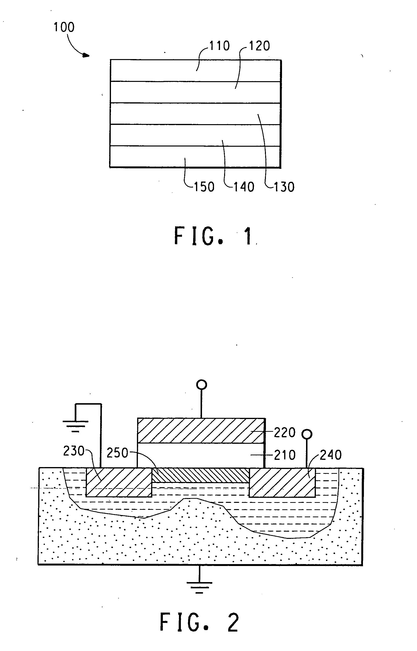
Compositions are provided comprising aqueous dispersions of electrically conducting organic polymers and a plurality of nanoparticles. Invention compositions are capable of providing continous, smooth thin films as buffer layers in electroluminescent devices, such as organic light emitting diodes (OLEDs) or as electrodes for thin film field effect transistors. Nanoparticles contemplated for use in the practice of the invention can be inorganic or organic. Buffer layers containing inorganic or organic nanoparticles have a much lower conductivity than buffer layers without such nanoparticles. When incorporated into an electroluminescent (EL) device, buffer layers according to the invention provide high resistance while contributing to higher stress life of the EL device.
In accordance with a further embodiment of the invention, there are provided methods for reducing the conductivity of an electrically conductive organic polymer film cast from an aqueous dispersion of an electrically conducting polymer onto a substrate, comprising adding a plurality of nanoparticles to the aqueous dispersion.
In a still further embodiment of the invention, there provided methods for increasing conductivity of thin film field effect transistor electrodes cast from aqueous dispersion onto a substrate.

Problems solved by technology

This is too high to avoid cross-talk between pixels.

Method used


Image

  • Electrically conducting organic polymer/nanoparticle composites and methods for use thereof
  • Electrically conducting organic polymer/nanoparticle composites and methods for use thereof
  • Electrically conducting organic polymer/nanoparticle composites and methods for use thereof

Examples


invention example 1

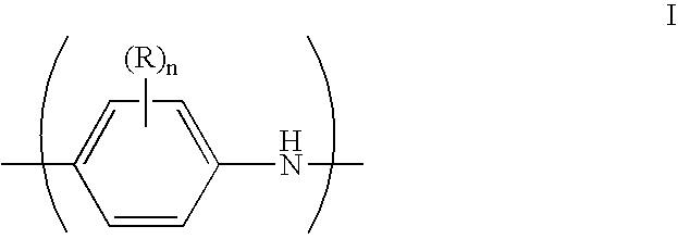
This example illustrates preparation of an aqueous PAni / PAAMPSA dispersion with silica nanoparticles and its electrical conductivity and light emission properties as a buffer layer.

PAni / PAAMPSA (0.63 g) prepared as in Comparative Example 1 was combined with 0.75 g Snowtex-UP® (0.75 g, Nissan Chemical Industries, Ltd. Tokyo, Japan), which contains 0.152 g silica nanoparticles, and 24.07 g deionized water. Snowtex-UP® is an aqueous dispersion having a pH from 9.0 to 10.5, and having a silica particle size of about 5-20 nm in width and about 40-300 nm in length. The silica:PAni / PMMPSA weight ratio is 4.1:1.

The dispersion was tested for electrical conductivity and light emission properties in the same manner as described in Comparative Example 1. As shown in the results summarized in Table 1, a buffer layer cast from the dispersion of Invention Example 1 has a lower conductivity (8.2×10⁻⁷ S / cm vs. 3.6×10⁻⁵ S / cm) and higher half-life (29 hours vs. 12 hours) when compared with Compar...

invention example 2

This example illustrates preparation of an invention aqueous PAni / PAAMPSA dispersion with colloidal silica and its electrical conductivity and light emission properties as a buffer layer.

PAni / PMMPSA (0.61 g) as prepared in Comparative Example 1 was combined with Snowtex-O® (0.75 g, from Nissan Chemical Industries, Ltd. Tokyo, Japan), which contains 0.153 g silica nanoparticles, and 23.47 g deionized water. Snowtex-O® is an aqueous dispersion having a pH range of 2-4 and having a silica particle size of 10-20 nm. The silica:PAni / PAAMPSA weight ratio is 3.99:1.

The dispersion was tested for electrical conductivity and light emission properties in the same manner as described in Comparative Example 1. As shown in the results summarized in Table 1, a buffer layer cast from the dispersion of Invention Example 2 has a lower conductivity (7.6×10⁻⁷ S / cm vs. 3.6×10⁻⁵ S / cm) and higher half-life (30 hours vs. 12 hours) when compared with Comparative Example 1. This example again demonstrat...

invention example 3

This example illustrates preparation of an invention aqueous PAni / PAAMPSA dispersion with electrically semi-conductive oxide and its electrical conductivity and light emission properties as a buffer layer.

PAni / PAAMPSA (0.90 g) as prepared in Comparative Example 1 was combined with Celnax CX-Z300H® (1.97 g, a zinc antimonite from Nissan Chemical Industries, Ltd. Tokyo, Japan), which contains 0.601 g conductive oxide particles, and 48.53 g deionized water. The Celnax CX-Z300H® is an aqueous dispersion having a pH of 6.85, and having 20 nm oxide nanoparticles. Conductivity of the oxide powder is 3.6 S / cm measured on a compressed dried pellet at a pressure of 160 Kg / cm2. The oxides:PAni / PAAMPSA weight ratio is 1.50:1.

The dispersion was tested for electrical conductivity and light emission properties in the same manner as described in Comparative Example 1. As shown in the results summarized in Table 1, a buffer layer cast from the dispersion of Invention Example 3 has a lower condu...


PUM

PropertyMeasurementUnit
Electrical conductivityaaaaaaaaaa
Particle sizeaaaaaaaaaa

Abstract

Compositions are provided comprising aqueous dispersions of electrically conducting organic polymers and a plurality of nanoparticles. Films cast from invention compositions are useful as buffer layers in organic electronic devices, such as organic light emitting diodes (OLEDs) and electrodes for thin film field effect transistors. Buffer layers containing nanoparticies have a much lower conductivity than buffer layers without nanoparticles. In addition, when incorporated into an electroluminescent (EL) device, buffer layers according to the invention contribute to higher stress life of the EL device.

Description

FIELD OF THE INVENTION The invention relates to the use of conductive organic polymers in the production of pixellated electroluminescent devices, such as organic light emitting diodes, and thin film field effect transistor electrodes. BACKGROUND Conductive organic polymers originally attracted the attention of researchers over 20 years ago. The interest generated by these polymers compared to conventional conducting materials (e.g., metals, semiconductive metal oxides) was largely due to factors such as light weight, flexibility, durability, and potential ease of processing. To date the most commercially successful conductive organic polymers are the polyanilines and polythiophenes, which are marketed under a variety of tradenames. These materials can be prepared by polymerizing aniline or dioxythiophene monomers in aqueous solution in the presence of a water soluble polymeric acid, such as poly(styrenesulfonic acid) (PSS), as described in, for example, U.S. Pat. No. 5,300,575 en...

Claims


Application Information

Patent Timeline
IPC IPC(8): C08K3/00C09D7/61C09D7/65H01B1/12H01L33/00H01L33/12H01L33/26H01L51/00H01L51/05H01L51/30H01L51/40H01L51/50
CPCB82Y10/00Y02E10/549B82Y30/00C01P2004/13C01P2004/16C01P2004/54C01P2004/62C01P2004/64C01P2006/40C08K3/0008C08K3/04C08K3/08C08K7/06C08K7/24C08K2201/011C08L25/18C08L33/24C08L65/00C08L79/02C09C1/0081C09D5/028C09D5/24C09D7/1216C09D7/1266C09D7/1275C09D7/1291H01B1/12H01L51/0021H01L51/0035H01L51/0037H01L51/0048H01L51/0052H01L51/0541H01L51/0566H01L51/5088H01L2251/5369B82Y20/00C08L2666/06C08L2666/14C08L2666/22C09D7/61C09D7/67C09D7/68C09D7/70C08K3/01C09D7/65H10K71/60H10K85/111H10K85/1135H10K85/221H10K85/615H10K10/488H10K10/464H10K50/17H10K2102/331C09K11/06B82B3/00
Inventor HSU, CHE-HSIUNG
Owner LG CHEM LTD
Learn More