
Method of manufacturing electronic component, method of manufacturing electro-optical device, electronic component, and electro-optical device

a manufacturing method and technology of electronic components, applied in the direction of non-linear optics, radio frequency controlled devices, instruments, etc., can solve the problems of difficult alignment of bump electrodes of the ic chip and the conductive pads of the circuit board, increase the cost of acf, and take time to inject underfill resin

Inactive Publication Date: 2005-03-31
SEIKO EPSON CORP
View PDF3 Cites 5 Cited by
  • Summary
  • Abstract
  • Description
  • Claims
  • Application Information

AI Technical Summary

Benefits of technology

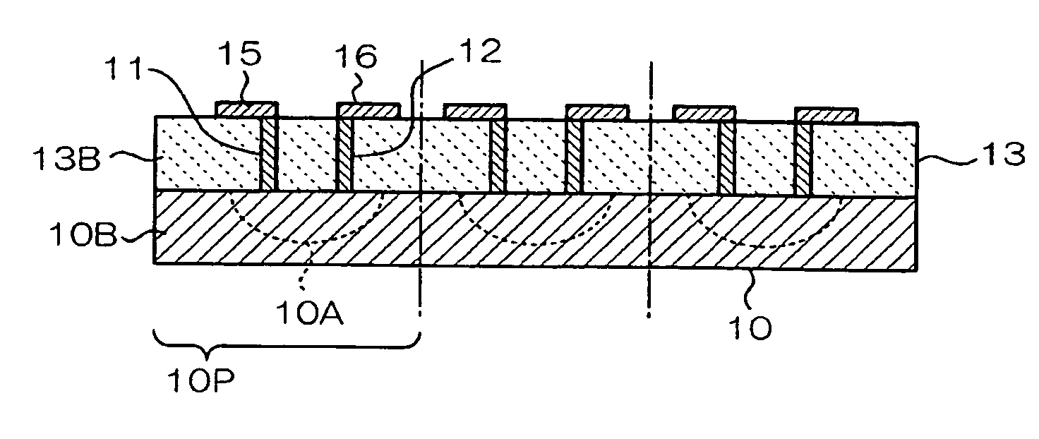
[0049] In this method, the thermoplastic resin layer is formed on the surface of the semiconductor substrate so that the bump electrode is buried; the conductive pattern electrically connected to the bump electrode is formed on the surface of the thermoplastic resin layer opposite to the semiconductor substrate; and the semiconductor substrate is divided in units of the integrated circuits. Therefore, since the thermoplastic resin and the conductive patterns can be formed collectively while the integrated circuits are integrally formed on the semiconductor substrate, the electronic component can be efficiently manufactured, whereby the manufacturing cost can be reduced. Moreover, since the conductive pattern can be formed on the basis of the single semiconductor substrate which shows a dimensional change due to a temperature change smaller than that of the thermoplastic resin, alignment can be facilitated and the positional accuracy of the conductive pattern can be improved, whereby electrical reliability can be secured. As the semiconductor substrate in this embodiment, a semiconductor wafer before being divided into semiconductor IC chips, a ceramic substrate before being divided into semiconductive ceramic capacitor, and the like can be given. The thermoplastic resin layer in this embodiment may be integrally formed on the semiconductor substrate, or may be formed in a state of divided pieces. In the latter case, the thermoplastic resin layer may be formed in a state in which the thermoplastic resin layer is divided in units of the integrated circuits.
[0057] By previously providing conductive material over the entire surface of the thermoplastic resin layer or in a range larger than the bump electrode, the bump electrode can be securely caused to be electrically connected to the conductive material. The conductive material can be patterned into a conductive pattern having a desired shape or pattern in the step of forming the conductive pattern. Therefore, alignment in the step of forming the thermoplastic resin layer can be made easier than the case of forming a conductive pattern on the surface of the thermoplastic resin layer.

Problems solved by technology

However, in the method of filling the space between the electronic component and the circuit board with the underfill resin, it may take time to inject the underfill resin.
In the mounting method using the ACF, since the conductive particles must be reduced in size as the pitch between the terminals is reduced, the cost of the ACF may be increased.
The method disclosed in Japanese Patent Application Laid-open No. 2003-124259 may make it difficult to align the bump electrodes of the IC chip and the conductive pads of the circuit board.

Method used


Image

  • Method of manufacturing electronic component, method of manufacturing electro-optical device, electronic component, and electro-optical device
  • Method of manufacturing electronic component, method of manufacturing electro-optical device, electronic component, and electro-optical device
  • Method of manufacturing electronic component, method of manufacturing electro-optical device, electronic component, and electro-optical device

Examples


first embodiment

[0098] First Embodiment

[0099] The first embodiment according to the present invention is described below with reference to FIGS. 1A to 1C. In this embodiment, as shown in FIG. 1A, a semiconductor substrate 10 integrally provided with a plurality of integrated circuits 10A is provided. The semiconductor substrate 10 may be a semiconductor substrate which is formed of a silicon single crystal, a compound semiconductor single crystal, or the like and includes a predetermined electronic circuit structure as the integrated circuit 10A. However, the semiconductor substrate 10 may be a ceramic substrate. The semiconductor substrate 10 is formed to a thickness of about 100 to 800 μm when the semiconductor substrate 10 is a semiconductor wafer, and is formed to a thickness of about 1 to 5 mm when the semiconductor substrate 10 is a ceramic stack.

[0100] In either case, the integrated circuits 10A are integrally formed in the semiconductor substrate 10. The integrated circuits 10A are arrange...

second embodiment

[0109] Second Embodiment

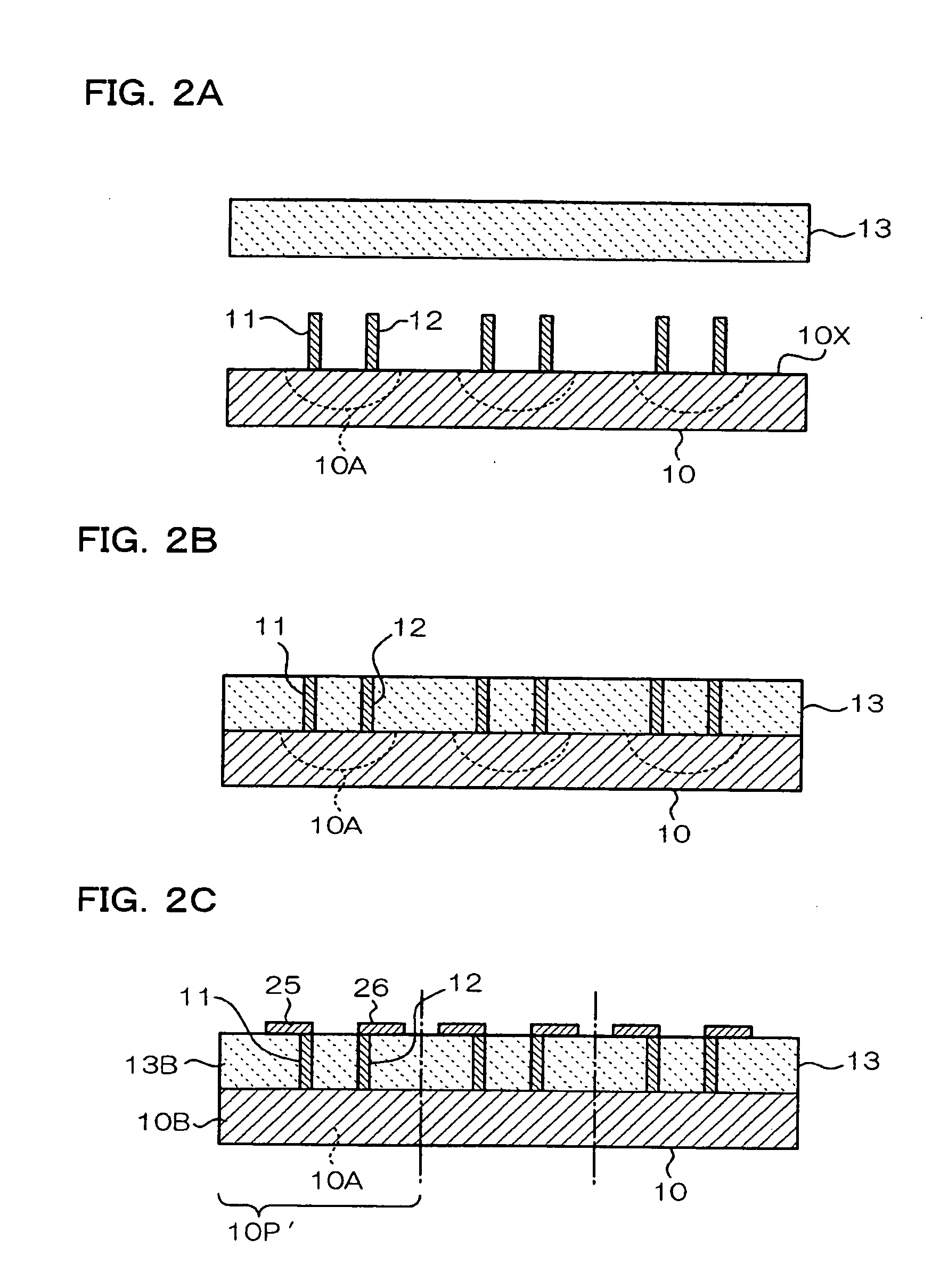
[0110] The second embodiment according to the present invention is described below with reference to FIGS. 2A to 2C and FIG. 6. In this embodiment, constituent elements the same as the constituent elements in the first embodiment are denoted by the same symbols. Description of these constituent elements is omitted. In this embodiment, as shown in FIG. 2A, the thermoplastic resin layer 13 is formed on the semiconductor substrate 10 by using the same method as in the first embodiment. However, in this embodiment, a conductor layer is not formed on the surface of the thermoplastic resin layer 13. As shown in FIG. 2B, in the step of forming the thermoplastic resin layer, the ends of the bump electrodes 11 and 12 are exposed from the surface of the thermoplastic resin layer 13 opposite to the semiconductor substrate 10.

[0111] As shown in FIG. 2C, conductors 25 and 26 are formed on the surface of the thermoplastic resin layer 13 so that the conductors 25 and 26 ar...

third embodiment

[0123] Third Embodiment

[0124] The third embodiment according to the present invention is described below with reference to FIGS. 4A to 4C. In this embodiment, constituent elements the same as the constituent elements in the first embodiment or the second embodiment are denoted by the same symbols. Description of these constituent elements is omitted.

[0125] In this embodiment, a thermoplastic resin layer is formed on the mounting surface 10X of the semiconductor substrate 10 by molding. In more detail, the semiconductor substrate 10 is placed in a die so that a cavity C is disposed on the mounting surface 10X of the semiconductor substrate 10 as indicated by one-dot lines shown in FIG. 4A, and a molten resin is injected into the cavity C as indicated by the arrow by using an injection molding machine (not shown) or the like. The injected resin is cured due to a decrease in the temperature inside the die, whereby a thermoplastic resin layer 23 shown in FIG. 4B is formed.

[0126] In th...


PUM

PropertyMeasurementUnit
thicknessaaaaaaaaaa
thicknessaaaaaaaaaa
diameteraaaaaaaaaa

Abstract

A method of manufacturing an electronic component, including: forming a thermoplastic resin layer on a surface of a semiconductor substrate including a plurality of integrated circuits and a bump electrode provided on each of the integrated circuits, to bury the bump electrode; forming a conductive pattern on a surface of the thermoplastic resin layer opposite to the semiconductor substrate, and electrically connecting the conductive pattern to the bump electrode; and dividing the semiconductor substrate in units of the integrated circuits.

Description

[0001] Japanese Patent Application No. 2003-297651, filed on Aug. 21, 2003, and Japanese Patent Application No. 2004-69556, filed on Mar. 11, 2004, are hereby incorporated by reference in their entirety. BACKGROUND OF THE INVENTION [0002] The present invention relates to a method of manufacturing an electronic component, a method of manufacturing an electro-optical device, an electronic component, and an electro-optical device. [0003] In various types of electronic instruments, an electronic component such as a semiconductor IC is generally mounted on a circuit board or the like to make up a part of an electronic circuit. As a method for mounting an electronic component on a circuit board or the like, various methods have been proposed. For example, a mounting method in which bump electrodes of an electronic component are bonded to conductive pads on a circuit board and the space between the electronic component and the circuit board is filled and sealed with an underfill resin has ...

Claims


Application Information

Patent Timeline
Patent Type & Authority Applications(United States)
IPC IPC(8): G02F1/13H05K3/32G02F1/1345H01L21/00H01L21/56H01L21/60H01L23/12H01L23/31H01L23/48H05K3/00
CPCH01L21/56H01L2924/12041H01L24/03H01L24/11H01L24/12H01L24/16H01L2224/03505H01L2224/0401H01L2224/13099H01L2924/01002H01L2924/01013H01L2924/01015H01L2924/01027H01L2924/01029H01L2924/0103H01L2924/01033H01L2924/01047H01L2924/01075H01L2924/01079H01L2924/09701H01L2924/12044H01L2924/14H01L2924/19041H01L2924/01005H01L2924/01006H01L2924/0105H01L23/3114H01L2924/15787H01L2924/12042H01L2924/00G02F1/1345
Inventor SAITO, ATSUSHI
Owner SEIKO EPSON CORP
Learn More