
Thin film transistor and fabrication method for same

a technology of thin film transistors and fabrication methods, applied in non-linear optics, instruments, optics, etc., can solve the problems of increasing costs and lowering throughput and yield, increasing cost and increasing cost, and difficulty in etching uneven surfaces, so as to reduce photolithography steps, avoid alignment errors, and improve yield

Inactive Publication Date: 2005-03-17
CHINA STAR OPTOELECTRONICS INT HK
View PDF1 Cites 5 Cited by
  • Summary
  • Abstract
  • Description
  • Claims
  • Application Information

AI Technical Summary

Benefits of technology

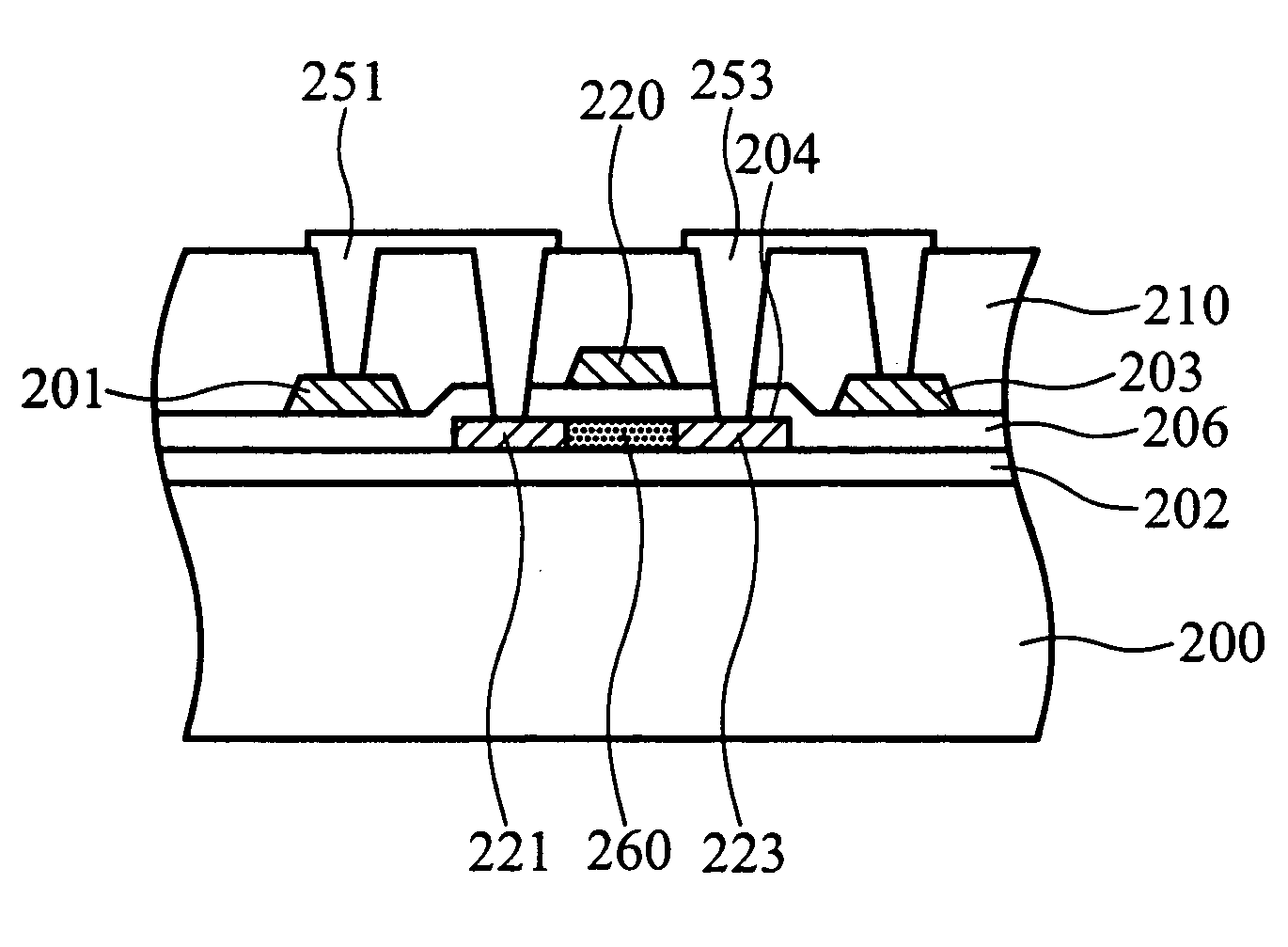
[0022] Accordingly, an object of the present invention is to provide a thin film transistor. In the crystalline silicon TFT manufacturing process of the present invention, the gate electrodes act as masks and the source / drain regions are formed using a self-aligned implantation process, and the dielectric layer is defined to form all contact holes through a photolithography step thus eliminating the problem of different contact hole opening heights in the dielectric layer. Moreover, the scan lines and data lines are simultaneously defined in one photolithography step. The present invention only employs four photolithography steps to manufacture the crystalline silicon TFT as described, thereby reducing the photolithography steps of conventional process and avoiding alignment errors, further improving yield and increasing throughput.
[0024] Yet another object of the invention is to provide a method of fabricating a thin film transistor for a transflective display, only requiring five photolithography steps to manufacture the above TFT, and further simplify the process of fabricating a switchable transflective display.
[0025] Still another object of the invention is to provide a method of fabricating a CMOS thin film transistor with lightly doped drain structure, only requiring six photolithography steps to manufacture the above TFT, further simplifying the conventional fabricating process.

Problems solved by technology

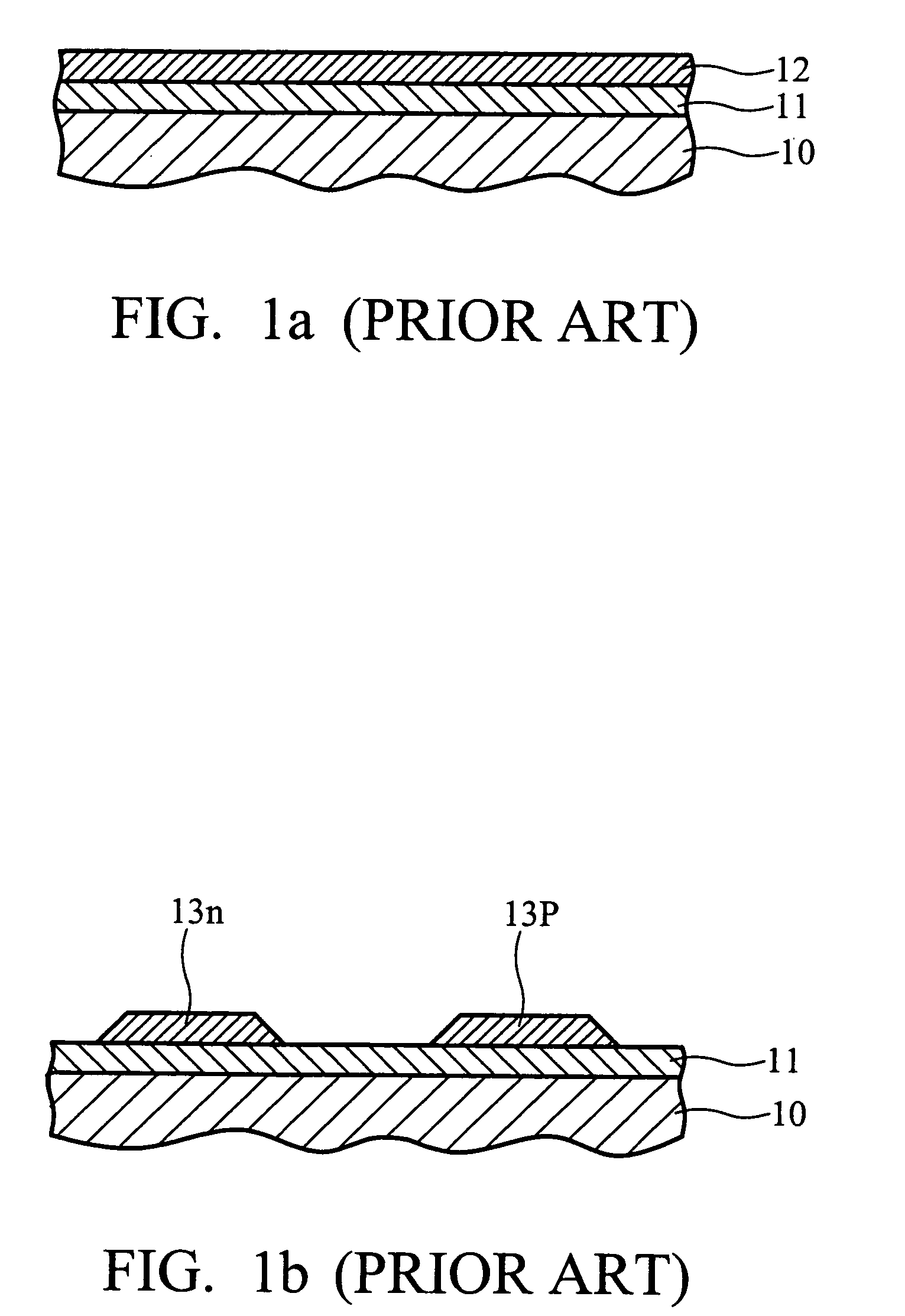
Compared to the number of process steps required to form an amorphous silicon TFT, however, more process steps are required to form crystalline silicon TFT hence, the process is more complicated and time-consuming.
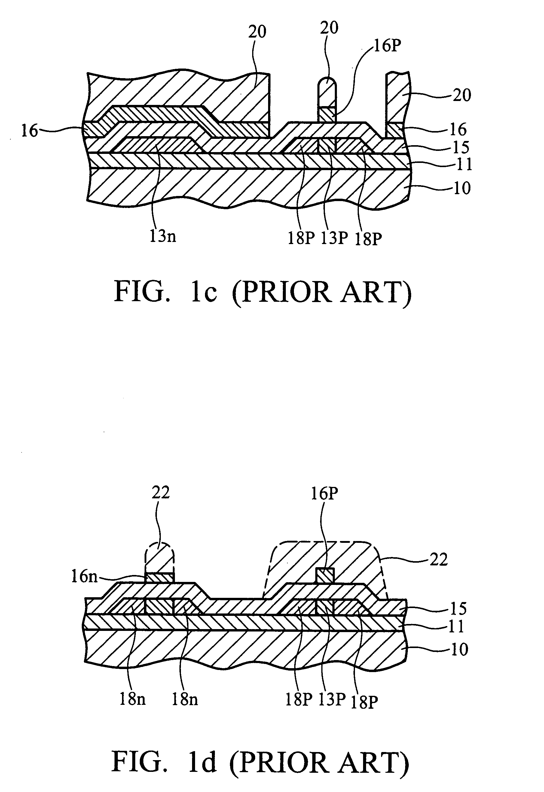
The conventional fabrication method described above requires nine photolithography steps, which increases costs and lowers throughput and yield.
The opening of each contact hole, however, is at a different height and etching the uneven surface is difficult.
That is, the narrow process window of the conventional crystalline silicon TFT increases the difficulty of manufacturing.
Additionally, the crystallization process window is limited as a result of the metal lines formed prior to crystallization.
However, the process window of this manufacturing process is also limited due to the harsher requirements of tape angles of the source / drain electrodes and complicated crystallization.

Method used


Image

  • Thin film transistor and fabrication method for same
  • Thin film transistor and fabrication method for same
  • Thin film transistor and fabrication method for same

Examples


first embodiment

[0056]FIGS. 3a to 3g show the steps of a method of fabricating a thin film transistor according to the first embodiment of the present invention, wherein the method requires only-four photolithography steps.

[0057] First, referring to FIG. 3a, a substrate 200 is provided. A buffer layer 202 and a semiconductive layer are then formed on the substrate 200. Next, the semiconductive layer is defined to form a semiconductor island 204 by a first photolithography step, wherein the semiconductor island comprises a channel region 260 and predetermined source and drain regions 262 adjacent to the channel region 260.

[0058] Suitable material for the buffer layer 202 is a silicide, such as silicon nitride. Preferably, the semiconductive layer is a crystalline silicon layer, and methods of forming the crystalline silicon layer are unlimited in the present invention. For example, the method of forming the crystalline silicon layer comprises depositing an amorphous silicon layer followed by therm...

second embodiment

[0068]FIGS. 4a to 4g show the steps of a method of fabricating a thin film transistor for a transflective display according to the second embodiment of the present invention, wherein the method only employs five photolithography steps.

[0069] First, referring to FIG. 4a, a substrate 300 with a predetermined transmissive TFT region T and a predetermined reflective TFT region R is provided. A buffer layer 302 and a semiconductive layer are then formed on the substrate 300. Next, the semiconductive layer is defined to form a semiconductor island 304 on the predetermined transmissive TFT region and another on the predetermined reflective TFT region by a first photolithography step, wherein each semiconductor island comprises a channel region 360 and predetermined source and drain regions 362 adjacent to the channel region 360.

[0070] Suitable material for the buffer layer 302 is a silicide, such as silicon nitride. Preferably, the semiconductive layer is a crystalline silicon layer, and...

third embodiment

[0079]FIGS. 5a to 5g show the steps of a method of fabricating a CMOS thin film transistor with lightly doped drain structure according to the third embodiment of the present invention, wherein the method only employs six photolithography steps.

[0080] First, referring to FIG. 5a, a substrate 400 with a n-type MOS TFT region N, a p-type MOS TFT region P and an LDD region L is provided. Next, a buffer layer 402 and a semiconductive layer are formed on the substrate 400. The semiconductive layer is then patterned to form a first semiconductor island 404 on the LDD region L, a second semiconductor island 404p on the p-type MOS TFT region P, and the third semiconductor island 404n on the n-type MOS TFT region N respectively by a first photolithography step, wherein each of the second and third semiconductor islands comprise a channel region 460 and predetermined source and drain regions 462 adjacent to the channel region 460 and the first semiconductor island 404 comprises a channel reg...


PUM

PropertyMeasurementUnit
thicknessaaaaaaaaaa
thicknessaaaaaaaaaa
thicknessaaaaaaaaaa

Abstract

A thin film transistor and a method for fabricating the same. The thin film transistor comprises a substrate and a patterned semiconductive layer formed on the substrate, wherein the semiconductive layer comprises a channel region and doped regions adjacent to the channel region. A gate insulating layer is formed on the above structure. A gate electrode is located on the gate insulating layer above the channel region. Source and drain electrodes are located on the gate insulating layer adjacent to the semiconductive layer. A dielectric layer having contact holes is formed on the above structure and a patterned conductive layer is formed on predetermined parts of the dielectric layer electrically connecting the doped regions to the source and drain electrode through the contact holes.

Description

[0001] This application is a Divisional of co-pending application Ser. No. 10 / 651,009, filed on Aug. 29, 2003, and for which priority is claimed under 35 U.S.C. § 120; and this application claims priority of Application No. 092114697 filed in Taiwan, R.O.C. on May 30, 2003 under 35 U.S.C. § 119; the entire contents of all are hereby incorporated by reference.BACKGROUND OF THE INVENTION [0002] 1. Field of the Invention [0003] The present invention relates to a thin film transistor and fabricating method thereof. More particularly, the present invention relates to a thin film transistor and fabricating method thereof with fewer photolithography steps. [0004] 2. Description of the Related Art [0005] Thin film transistors (TFTs) drive pixels in active matrix type liquid crystal display devices, active matrix type organic light-emitting display devices, image sensors and the like. Generally, TFTs used in these apparatuses are formed from silicon semiconductor thin film. Such silicon semi...

Claims


Application Information

Patent Timeline
Patent Type & Authority Applications(United States)
IPC IPC(8): G02F1/1368H01L21/28H01L21/336H01L21/77H01L21/84H01L27/12H01L29/417H01L29/423H01L29/49H01L29/786H01L51/50
CPCH01L29/41733H01L27/1288H01L27/124H01L29/66757
Inventor CHEN, CHEN-MINGWU, YUNG-FU
Owner CHINA STAR OPTOELECTRONICS INT HK
Learn More