
How to form a CMOS transistor

A technology of transistors and semiconductors, applied in semiconductor/solid-state device manufacturing, electrical components, circuits, etc., can solve problems such as the complexity of fin CMOS transistor technology, and achieve the effects of saving photolithography steps, easy removal, and improving performance

Active Publication Date: 2016-06-29
SEMICON MFG INT (SHANGHAI) CORP
View PDF5 Cites 0 Cited by
  • Summary
  • Abstract
  • Description
  • Claims
  • Application Information

AI Technical Summary

Problems solved by technology

[0007] The problem solved by the present invention is that the process of forming stressful fin CMOS transistors in the prior art is complicated

Method used


Image

  • How to form a CMOS transistor
  • How to form a CMOS transistor
  • How to form a CMOS transistor

Examples


Embodiment Construction

[0033] It can be seen from the background art that in the prior art, in the process of forming a fin-type CMOS transistor with stress, in order to form the source and drain regions of NMOS and PMOS respectively, and to introduce stress in the channel region of NMOS and PMOS, it is necessary to use multiple The photolithography process is complex and costly.

[0034] The inventors of the present invention have studied the process of forming fin-type CMOS transistors in the prior art, and found that when doping the source and drain regions of NMOS in the prior art, it is necessary to form a mask layer covering the PMOS area by photolithography, and carry out N-type ion Implantation: When doping the source and drain regions of PMOS, photolithography is required to form a mask layer covering NMOS for P-type ion implantation. However, in order to introduce stress into the channel regions of the NMOS and PMOS transistors later, it is necessary to remove the source and drain regions ...


PUM


Abstract

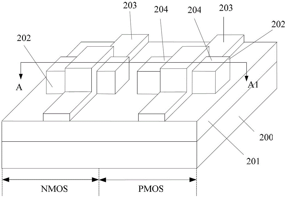
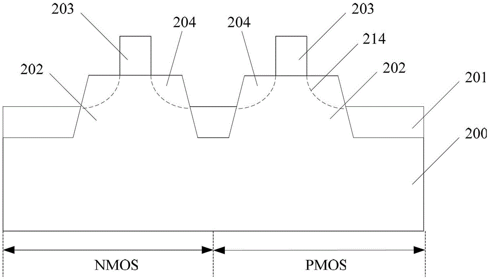
A forming method of a CMOS transistor comprises the steps that a semiconductor substrate is provided, and the semiconductor substrate comprises an NMOS area and a PMOS area; pre-decrystallization injection is conducted on the source region and the drain region of the NMOS area and the source region and the drain region of the PMOS area; the source region and the drain region of the NMOS area and the source region and the drain region of the PMOS area are etched to form a first opening, the depth of the first opening is smaller than the depth of pre-decrystallization injection, and an embedded source region and an embedded drain region of an NMOS are formed in the first opening; a blocking layer is formed, and the blocking layer is provided with a second opening exposing the PMOS area; the source region and the drain region of the PMOS area are etched along the second opening, the embedded source region and the embedded drain region of the NMOS and the pre-decrystallization injection area of the PMOS area are removed to form a third opening, and an embedded source region and an embedded drain region of the PMOS are formed in the third opening. The forming method of the CMOS transistor is simple in process.

Description

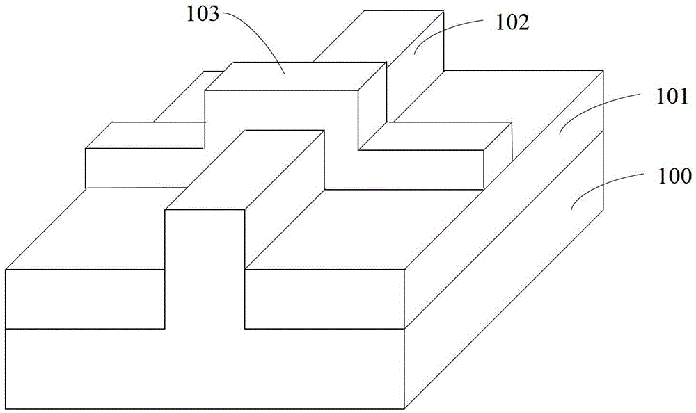
technical field [0001] The invention relates to the technical field of semiconductors, in particular to a method for forming a CMOS transistor. Background technique [0002] MOS transistors generate switching signals by regulating the current through the channel region by applying a voltage to the gate. However, when the semiconductor technology enters the node below 45 nanometers, the control ability of the traditional planar MOS transistor on the channel current becomes weak, causing serious leakage current. Fin Field Effect Transistor (FinFET) is an emerging multi-gate device, which generally includes a semiconductor fin with a high aspect ratio, a gate structure covering part of the top and sidewall of the fin, located on the gate Source and drain regions within the fins on either side of the structure. [0003] figure 1 A schematic diagram of a three-dimensional structure of a fin field effect transistor in the prior art is shown. The fin field effect transistor inc...

Claims


Application Information

Patent Timeline
Patent Type & Authority Patents(China)
IPC IPC(8): H01L21/8238
CPCH01L21/02219H01L21/02318H01L21/823814
Inventor 三重野文健
Owner SEMICON MFG INT (SHANGHAI) CORP
Learn More