Manufacturing method of LED chip electrode mask pattern capable of being directly stripped
A manufacturing method and an electrode technology, which are applied in the field of manufacturing LED die electrode mask patterns, can solve the problems of restricting large-scale use, cumbersome process, and easy generation of splits, and achieve low cost, simple process, and reduced photolithography. The effect of steps
Pending Publication Date: 2020-08-04
SHANDONG INSPUR HUAGUANG OPTOELECTRONICS
View PDF36 Cites 0 Cited by
- Summary
- Abstract
- Description
- Claims
- Application Information
AI Technical Summary
Problems solved by technology
The metal on the surface of the wafer is peeled off by high-pressure spraying, but the whole process is quite cumbersome. NMP high-pressure spraying has high requirements on the wafer substrate. When the wafer is thin, it is easy to produce cracks. In order to obtain higher brightness, the Generally only do less than 150 microns, so this has limited the wide range of use of the invention
Method used
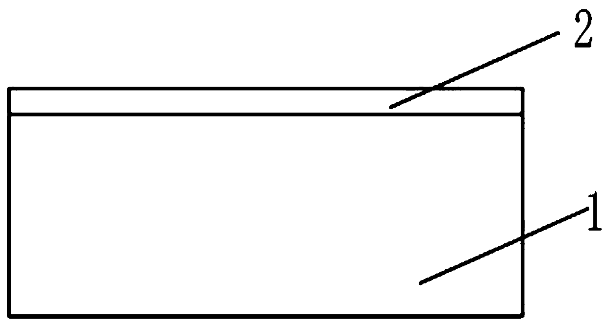
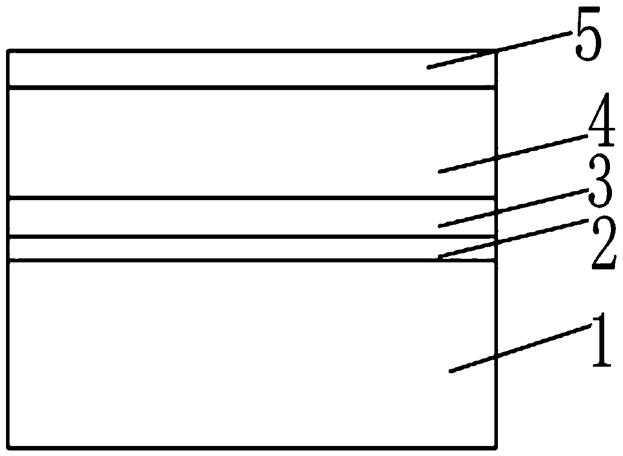
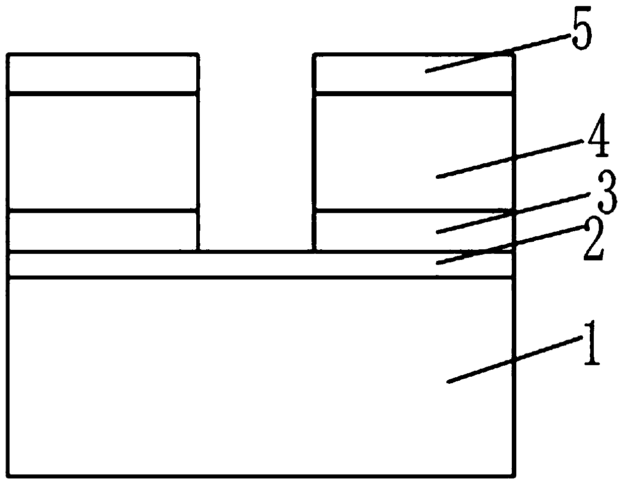
View moreImage
Smart ImageViewing Examples
Examples
Embodiment 2
[0040] The temperature in the growth chamber of the PECVD equipment in step b) is 60-90°C.
Login to View More PUM
| Property | Measurement | Unit |
|---|---|---|
| thickness | aaaaa | aaaaa |
| thickness | aaaaa | aaaaa |
Abstract
The invention discloses a manufacturing method of an LED chip electrode mask pattern capable of being directly stripped. Two adhesive film layers formed by negative photoresist and a filling layer arranged between a first adhesive film layer and a second adhesive film layer are prepared on an LED crystal to obtain the suitable metal electrode mask pattern; the first adhesive film layer and the second adhesive film layer are thinner, so that the mask pattern meeting thicker requirements is manufactured by using less photoresist, the obtained metal electrode pattern can be directly subjected tometal tearing stripping on the premise of completeness, and additional treatment is not needed. Through cooperation of the two photoresist layers and a silicon dioxide layer with proper thicknesses, the effect of directly stripping the metal electrode mask pattern which can only be manufactured by using thick adhesive can be achieved; the first adhesive film layer, the filling layer and the secondadhesive film layer are sequentially manufactured, and then the electrode mask pattern is prepared, so that two photoetching steps can be reduced, the whole process is simple and easy to implement, and the cost is relatively low.
Description
technical field [0001] The invention relates to the technical field of LED manufacturing, in particular to a method for making a mask pattern of an LED tube core electrode that can be directly peeled off. Background technique [0002] Light Emitting Diode, referred to as LED (Light Emitting Diode), is a solid-state electroluminescent (EL) semiconductor device that converts electrical energy into light energy. The substantial core structure of the LED is a P-N section composed of III-IV or III-V compound materials in the element spectrum. The spectral distribution of LED light radiation has its unique side. It is not monochromatic light (such as a laser), nor is it a broad-spectrum radiation (such as an incandescent lamp), but somewhere in between, with a bandwidth of tens of nanometers and a peak wavelength in the visible or near-infrared region. Compared with ordinary light sources, LED has the following advantages: 1. High efficiency: high luminous efficiency, LED lamps ...
Claims
Login to View More Application Information
Patent Timeline
 Patent Type & Authority Applications(China)
IPC IPC(8): G03F7/095G03F7/11G03F7/16H01L21/027H01L33/00
CPCG03F7/095G03F7/11G03F7/168H01L21/0272H01L33/005
Inventor 徐晓强张兆喜吴向龙闫宝华王成新
Owner SHANDONG INSPUR HUAGUANG OPTOELECTRONICS
Features
- R&D
- Intellectual Property
- Life Sciences
- Materials
- Tech Scout
- Unparalleled Data Quality
- Higher Quality Content
- 60% Fewer Hallucinations
Learn More Browse by: Latest US Patents, China's latest patents, Technical Efficacy Thesaurus, Application Domain, Technology Topic, Popular Technical Reports.
© 2025 PatSnap. All rights reserved.Legal|Privacy policy|Modern Slavery Act Transparency Statement|Sitemap|About US| Contact US: help@patsnap.com


