Method of fabricating low temperature polysilicon thin film transistor

Inactive Publication Date: 2005-03-17
INNOLUX CORP
View PDF2 Cites 14 Cited by
  • Summary
  • Abstract
  • Description
  • Claims
  • Application Information

AI Technical Summary

Benefits of technology

[0015] It is an advantage of the claimed invention that the method forms a silicon nitride layer to increase the protective ability against moisture and metal ions and to provide a hydrogen source, and then forms a TEOS based silicon oxide layer to provide a good step coverage ability and reduce the dielectric constant of the composite inter-layer dielectric layer for avoiding the presence of parasitic capacitors. Thus, the electric performance and the stability of the low temperature polysilicon thin film transistor can be improved effectively.

Problems solved by technology

However, current materials used for the dielectric layer cannot meet these two requirements at the same time.
However, the silicon nitride layer also readily generates parasitic capacitors because of its high dielectric constant, leading to signal delay that is unsuitable for an interlayer dielectric layer.
However, its protection ability is much worse than the silicon nitride layer, as it cannot protect electric devices disposed beneath.
However, it has a low step coverage ability so that voids occur easily in the deposition process.
The latter has a good step coverage ability in the deposition process, but cannot serve as a hydrogen source.
This means that a subsequent hydrogen process is needed for an additional hydrogen source requiring much more equipment and manufacturing time.
As mentioned above, among all conventional methods, none can successfully make an interlayer dielectric layer that has a good interface characteristic, high threshold voltage stability, good protective ability against moisture and metal ions, and high break-down voltage.

Method used


Image

  • Method of fabricating low temperature polysilicon thin film transistor
  • Method of fabricating low temperature polysilicon thin film transistor
  • Method of fabricating low temperature polysilicon thin film transistor

Examples


first embodiment

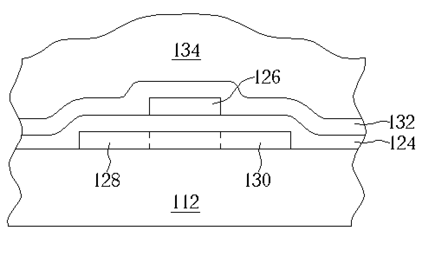
[0020] Please refer to FIG. 5 to FIG. 9, which are schematic diagrams offabricating an interlayer dielectric layer of a low temperature polysilicon thin film transistor according the present invention. As mentioned above, though a display panel normally comprises a plurality of low temperature polysilicon thin film transistors, only one low temperature polysilicon thin film transistor is illustrated in the following diagrams for clarity. As shown in FIG. 5, a display panel 110 comprises a substrate 112 on the surface thereof. The substrate 112 is a glass substrate or a silicon substrate. A chemical vapor deposition process or a sputtering process is performed to form an amorphous silicon film (not shown) with a thickness of 500 angstrom on a display panel 110. An excimer laser annealing process follows to make the amorphous silicon film crystallize to a polysilicon film 114. Then, a first photo-etching process is performed to pattern the polysilicon film and leave a predetermined po...

second embodiment

[0029] Please refer to FIG. 10 to FIG. 12, which are schematic diagrams offabricating an interlayer dielectric layer of a low temperature polysilicon thin film transistor according the present invention. As shown in FIG. 10, first, a gate 214 is formed on a substrate 212. Then, a gate insulating layer 216 and an amorphous silicon film 218 are formed on the gate 214 and the substrate 212 in sequence. Next, as shown in FIG. 11, an excimer laser annealing process is performed to make the amorphous silicon film 218 melted and crystallize to a polysilicon film 220. An ion implantation process is performed thereafter to form a source 222 and a drain 224 in the polysilicon film 220 to form a bottom gate type of a low temperature polysilicon thin film transistor 226. As shown in FIG. 12, in the same manner, a silane based silicon nitride layer 228 and a TEOS based silicon oxide layer 230 forms a composite interlayer dielectric layer 232 positioned on the low temperature polysilicon thin fil...


PUM


Abstract

First, a substrate with a polysilicon film is provided. Then, a gate insulating layer and a gate are formed on the polysilicon film in sequence. An ion implantation process is performed to form a source and a drain around the gate. After that, a first plasma enhanced chemical vapor deposition (PECVD) process is performed to form a silicon nitride layer over the substrate and the gate. A second plasma enhanced chemical vapor deposition process is then performed to form a TEOS based silicon oxide layer on the silicon nitride layer. A photo-etching process follows to form a contact hole extending through to the source and drain respectively. Then, a conductive layer is filled into the contact holes and electrically connected to the source and drain.

Description

BACKGROUND OF INVENTION [0001] 1. Field of the Invention [0002] The present invention relates to a method of fabricating an interlayer dielectric layer (ILD) of a low temperature polysilicon thin film transistor, and more particularly, to a method of fabricating a low temperature polysilicon thin film transistor that has a composite interlayer dielectric layer. [0003]2. Description of the Prior Art [0004] Nowadays, liquid crystal displays (LCDs) are a mature flat panel display technology. Applications for liquid crystal displays are extensive, including devices such as mobile phones, digital cameras, video cameras, notebooks, and monitors. Due to high quality display requirements and expansion into new application fields, LCD technology is being developed toward high quality, high resolution, high brightness, and low cost. Actively driven low temperature polysilicon thin film transistors (LTPS TFTs) are a break-through toward achieving the above objectives. [0005] In the fabrication...

Claims


Application Information

Patent Timeline
IPC IPC(8): H01L21/336H01L21/77H01L21/84
CPCH01L29/66757H01L27/1248H01L29/66765
Inventor LIN, HUI-CHU
Owner INNOLUX CORP
Why Eureka
Try Eureka