Method of manufacturing an insulation film in a semiconductor device

Inactive Publication Date: 2002-01-03
HYUNDAI ELECTRONICS IND CO LTD
View PDF0 Cites 7 Cited by
  • Summary
  • Abstract
  • Description
  • Claims
  • Application Information

AI Technical Summary

Benefits of technology

0009] A method of manufacturing an insulating film in a semiconductor device is disclosed which is capable of solving the aforenoted problems. Specifically, a silicon oxide film is deposited to form a hard mask film, wherein the supply a

Problems solved by technology

As the distance between the conductive layer patterns becomes smaller, and as the capacitance between the patterns is increased, when a device is driven, the transfer of the signal is delayed, consumption of power is increased and a cross talk between lines is generated, thereby degrading the electrical characteristics of the device.
In this case, though the dielectric constant is reduced, a separation between the SOD film and the hard mask film occurs during a subsequent cleaning process since the adhesive force in the interface between the SOD film and the hard mask film becomes poor.

Method used


Image

  • Method of manufacturing an insulation film in a semiconductor device
  • Method of manufacturing an insulation film in a semiconductor device
  • Method of manufacturing an insulation film in a semiconductor device

Examples


first embodiment

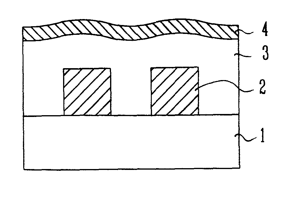
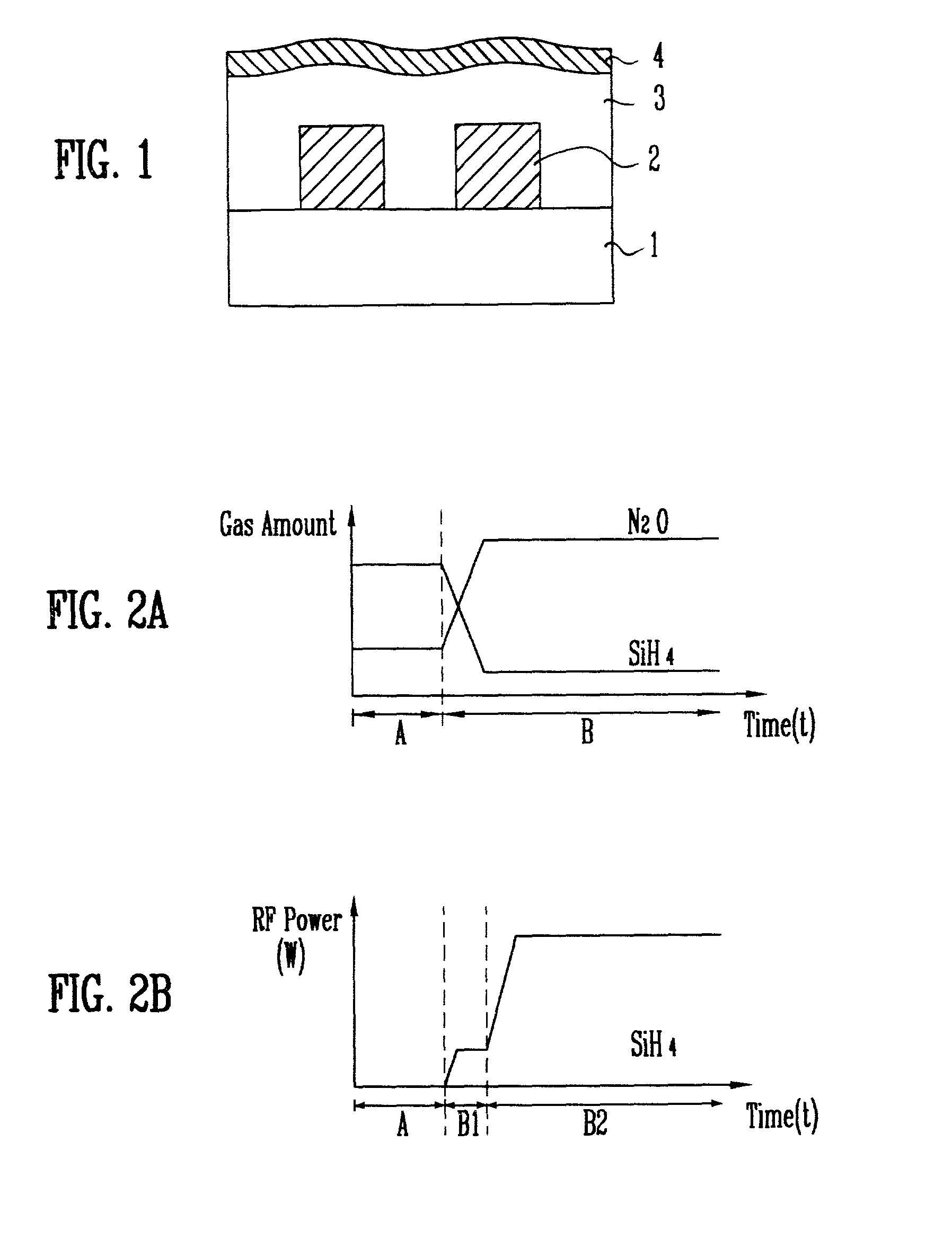
[0019] FIG. 1 is a cross-sectional view of a device for explaining a first embodiment, which will be explained by reference to FIGS. 2A and 2B.

[0020] After conductive layer patterns 2 are formed on a semiconductor substrate 1, a SOD film 3 is formed on the entire structure to fill the gap between the conductive patterns 2. At this time, the SOD film 3 may be formed of a polymer film of C, H, 0 components, a MSQ film or a HSQ film, wherein the gap between the conductive patterns 2 is completely filled by a high fluidity of the SOD film 3 and the degree of flatness in the surface of the conductive patterns 2 becomes better.

[0021] Thereafter, a curing process is performed in the reaction furnace at a temperature ranging from about 300.degree. C. to about 650.degree. C. Then, a silicon oxide film is formed on the SOD film 3 by plasma deposition method using SiH.sub.4 and N.sub.2O as a reaction gas under a low-temperature ranging from about 20.degree. C. to about 650.degree. C. and a low...

second embodiment

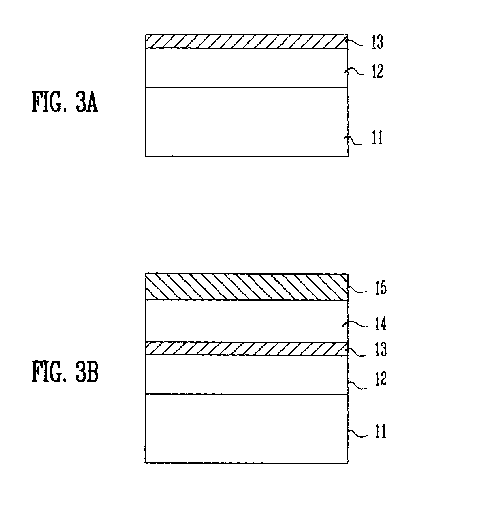
[0024] FIGS. 3A and 3B are cross-sectional views of a device for explaining the present invention, which will be explained by reference to FIGS. 2A and 2B again.

[0025] Referring to FIG. 3, a first SOD film 12 is formed on a semiconductor substrate 11 for which a given process is performed. Then, a curing process is performed at the temperature ranging from about 3000 to about 650.degree. C. Next, after a first hard mask film 13 is formed on the first SOD film 12 and a surface process is then performed in-situ. The surface process is performed by plasma, wherein the plasma employs a reaction gas such as N.sub.2, NH.sub.3, N.sub.2O, O.sub.2, Ar, He, etc. and is generated by supplying a RF power of a range from about of 10 W to about 100 W.

[0026] Referring to FIG. 3B, after a second SOD film 14 is formed on the first hard mask film 13 and is then experienced by a curing process, a second hard mask film 15 is formed on the second SOD film 14. The adhesive force of the first hard mask fi...


PUM

PropertyMeasurementUnit
Timeaaaaaaaaaa
Timeaaaaaaaaaa
Timeaaaaaaaaaa

Abstract

A method of manufacturing an insulating film in a semiconductor device is disclosed. The method comprises the steps of forming a SOD film on the entire structure to fill any distance between conductive layer patterns and after performing a curing process, forming a hard mask film on the SOD film, wherein the silicon oxide film is deposited by plasma deposition method using SiH4 and N2O as a reaction gas at a low-temperature and at a low-pressure and wherein in a stabilization step, the supply amount of SiH4 is greater than that of N2O and in a deposition step, the supply amount of N2O is greater than that of SiH4.

Description

[0001] 1. Field of the Invention[0002] The invention relates generally to a method of manufacturing an insulating film in a semiconductor device. More particularly, the present invention relates to a method of manufacturing an insulating film in a semiconductor device, capable of improving the adhesive force and reducing the dielectric constant, in a spin-on dielectric (SOD) film and a hard mask film.[0003] 2. Description of the Prior Art[0004] Generally, as a semiconductor device is highly integrated, the size of a conductive layer and the distance between the conductive layer patterns are reduced. As the distance between the conductive layer patterns becomes smaller, and as the capacitance between the patterns is increased, when a device is driven, the transfer of the signal is delayed, consumption of power is increased and a cross talk between lines is generated, thereby degrading the electrical characteristics of the device.[0005] Therefore, in order to prevent degradation of th...

Claims


Application Information

Patent Timeline
IPC IPC(8): H01L21/31C23C16/40C23C16/44C23C16/455H01L21/312H01L21/316H01L21/768H01L23/522H01L23/532
CPCC23C16/402C23C16/45523H01L21/02126H01L21/02164H01L21/022H01L21/02211H01L21/02274H01L21/02282H01L21/3121H01L21/3122H01L21/3124H01L21/31612H01L21/76826H01L21/76829H01L23/5329H01L2924/0002H01L2924/00H01L21/31
Inventor AHN, SANG TAESONG, JUNG GYU
Owner HYUNDAI ELECTRONICS IND CO LTD
Why Eureka
Try Eureka