
Patsnap Eureka
For R&D, Patsnap Eureka makes reading and utilizing patents & technical documents easy.
Patsnap Eureka AIR
Designed for self-driven R&D workflows. Generate viable solutions, solve complex R&D challenges, empower your innovation with AI.

Patsnap Eureka Materials
Designed for material experts only. Revolutionize your material R&D, from search, analyze, to developing new materials.

TechResearch
Generate reliable direction feasibility study reports for your R&D in just a few steps.

TechSeek
Discover and master advanced knowledge NOW. Basics, ideas, possibilities, all at once.

TechMind
As an expert in R&D Theories, TechMind can generates customized viable solutions instantly.

TechRisk
Analyze your overall solution with one click, know your potential R&D risks in advance.

TechMonitor
Get weekly tech updates, stay abreast of the latest tech innovations and key insights.
Silicon oxide co-deposition/etching process
- Summary
- Abstract
- Description
- Claims
- Application Information
AI Technical Summary
Benefits of technology
Problems solved by technology
Method used
Image

Examples
example
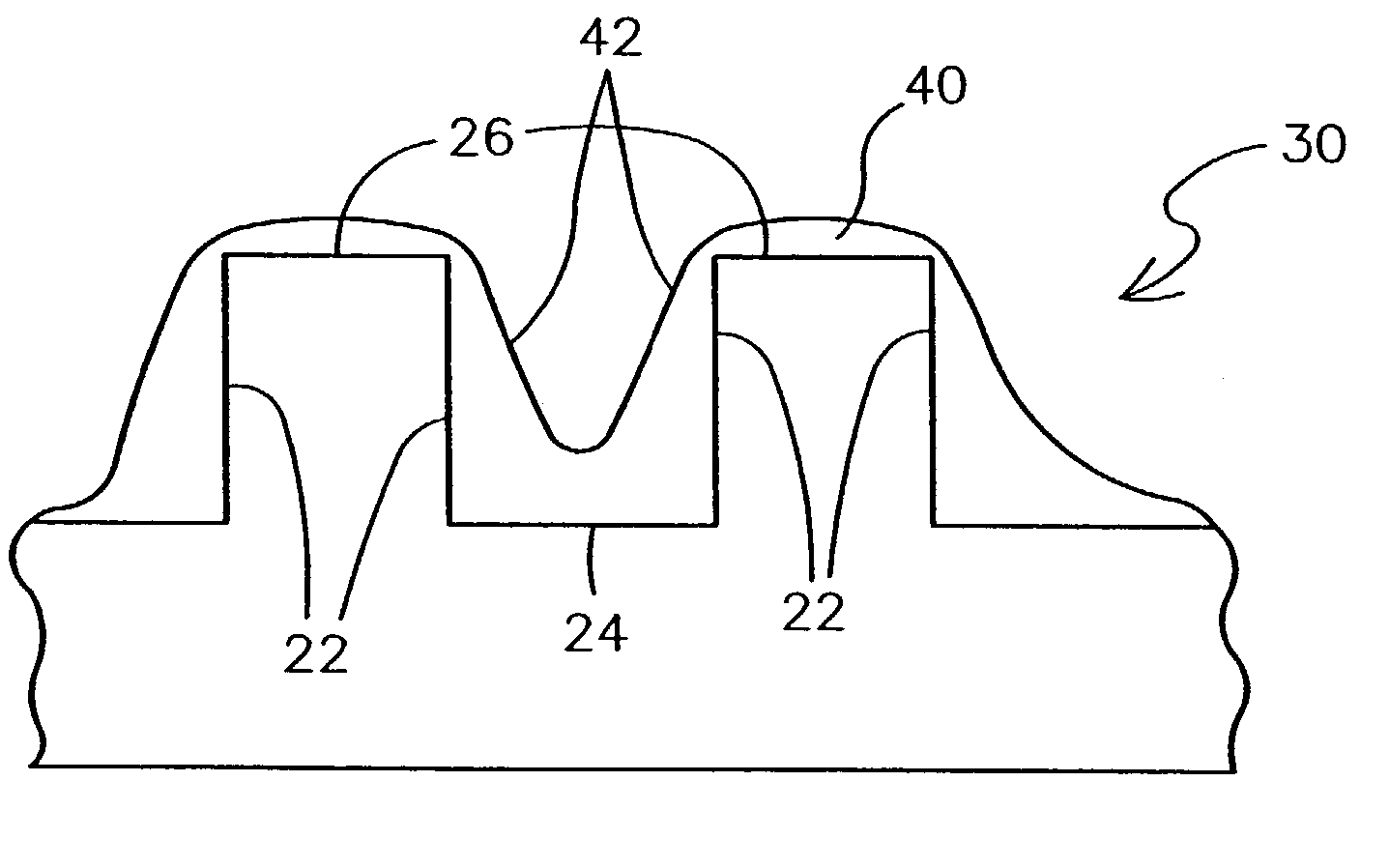
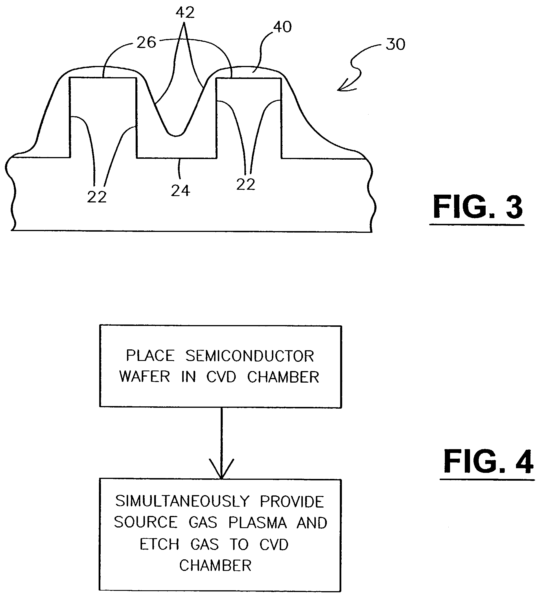
[0033]Features and advantages of the methods according to the present invention are further illustrated in the following example. It is recognized, however, that while the example serves this purpose, the particular process conditions, source and etch gases, and structures on which the silicon oxide is deposited, are not to be construed in a manner that would unduly limit the scope of this invention.
[0034]A silicon wafer substrate having word lines formed thereon was placed in CVD chamber. The pressure in the chamber was held at about 5×10⁻⁶ Torr and the temperature of the substrate was about 400° C. TEOS was introduced into the chamber at a rate of about 500 Standard Liters per Minute (slm) using a liquid injection system. The etch gas used was C2F6 and it was introduced into the chamber at the same time as the TEOS, but at a flow rate of 150 sccm. Both the source gas and the etch gas were excited by a plasma generator operating at 450 Watts. The source and etch gases were provided...
PUM
| Property | Measurement | Unit |
|---|---|---|
| Temperature | aaaaa | aaaaa |
| Time | aaaaa | aaaaa |
| Pressure | aaaaa | aaaaa |
Abstract
Description
Claims
Application Information
 - R&D Engineer
- R&D Manager
- IP Professional
- Industry Leading Data Capabilities
- Powerful AI technology
- Patent DNA Extraction
Browse by: Latest US Patents, China's latest patents, Technical Efficacy Thesaurus, Application Domain, Technology Topic, Popular Technical Reports.
© 2024 PatSnap. All rights reserved.Legal|Privacy policy|Modern Slavery Act Transparency Statement|Sitemap|About US| Contact US: help@patsnap.com