Method of forming an electrical isolation associated with a wiring level on a semiconductor wafer

Inactive Publication Date: 2007-11-15
INFINEON TECH AG
View PDF10 Cites 14 Cited by
  • Summary
  • Abstract
  • Description
  • Claims
  • Application Information

AI Technical Summary

Benefits of technology

[0008] In various embodiments, the present invention reduces the effects of capacitive or inductive coupling between wiring or metal lines of a wiring level of integrated circuits. A more particular embodiment reduces the mean dielectric constant k of the filling between different wiring levels. Further embodiments improve the manufacturing process and the quality of back-end of line (BEOL) process steps.
[0013] Further, it has been found that the PECVD process, if adapted to form voids within spacings by means of the deposition parameter settings, may be controlled such that a target geometry, size and position of the voids within the spacings can be maintained up to a considerable degree.
[0018] A further aspect of the invention relates to applying a second layer comprising a second dielectric material in addition to the first layer. Accordingly, the electrical isolation of the wiring level is provided by two different dielectric layers. Therein, the first layer formed by a PECVD process, which includes or leads to the formation of voids, mainly represents a so-called intrametal dielectric (IMD) layer. This layer serves to reduce capacitive and / or inductive coupling between wiring lines of the same wiring level. The second layer is provided as an interlevel dielectric (ILD) layer, which serves to reduce the capacitive and / or inductive coupling from wiring lines of one wiring level with respect to wirings lines of another wiring level.
[0019] In an alternate embodiment, a second layer comprising a second dielectric material is applied upon the first dielectric layer in order to yield a final passivation layer on top of a layer stack, which is formed upon a semiconductor wafer. This passivation layer serves to protect the chip underneath against mechanical or thermal stress. As this layer typically provides the uppermost layer on the substrate, no further metal layer is formed upon the passivation layer, disregarding possible wirings within a plastic chip housing, which may enclose the chip, and which may be bonded to the chip.
[0021] In a further embodiment relating to passivation layers, this layer may be constructed from amorphous carbon, solely. Herein, amorphous carbon is considered to provide both the air filled voids along with the ability to protect the chip underneath from mechanical or thermal influences.

Problems solved by technology

Several low-k materials are known, but the corresponding process integration requires large efforts and costs.
This is the reason why HDP deposition has been preferred over conventional plasma-enhanced CVD (PECVD: plasma enhanced chemical vapor deposition), since the deposition profile of PECVD-layers develops disadvantageous overhang sections due to the stronger growth of deposited material on horizontal surfaces as compared with vertical surfaces of structures on the wafer.
Further, the overhangs reveal an increased roughness at the surface.

Method used


Image

  • Method of forming an electrical isolation associated with a wiring level on a semiconductor wafer
  • Method of forming an electrical isolation associated with a wiring level on a semiconductor wafer
  • Method of forming an electrical isolation associated with a wiring level on a semiconductor wafer

Examples


Embodiment Construction

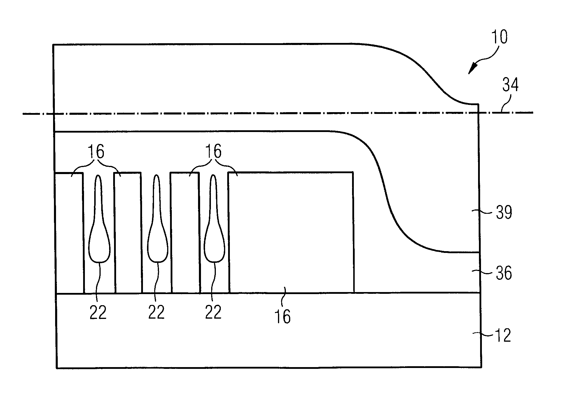
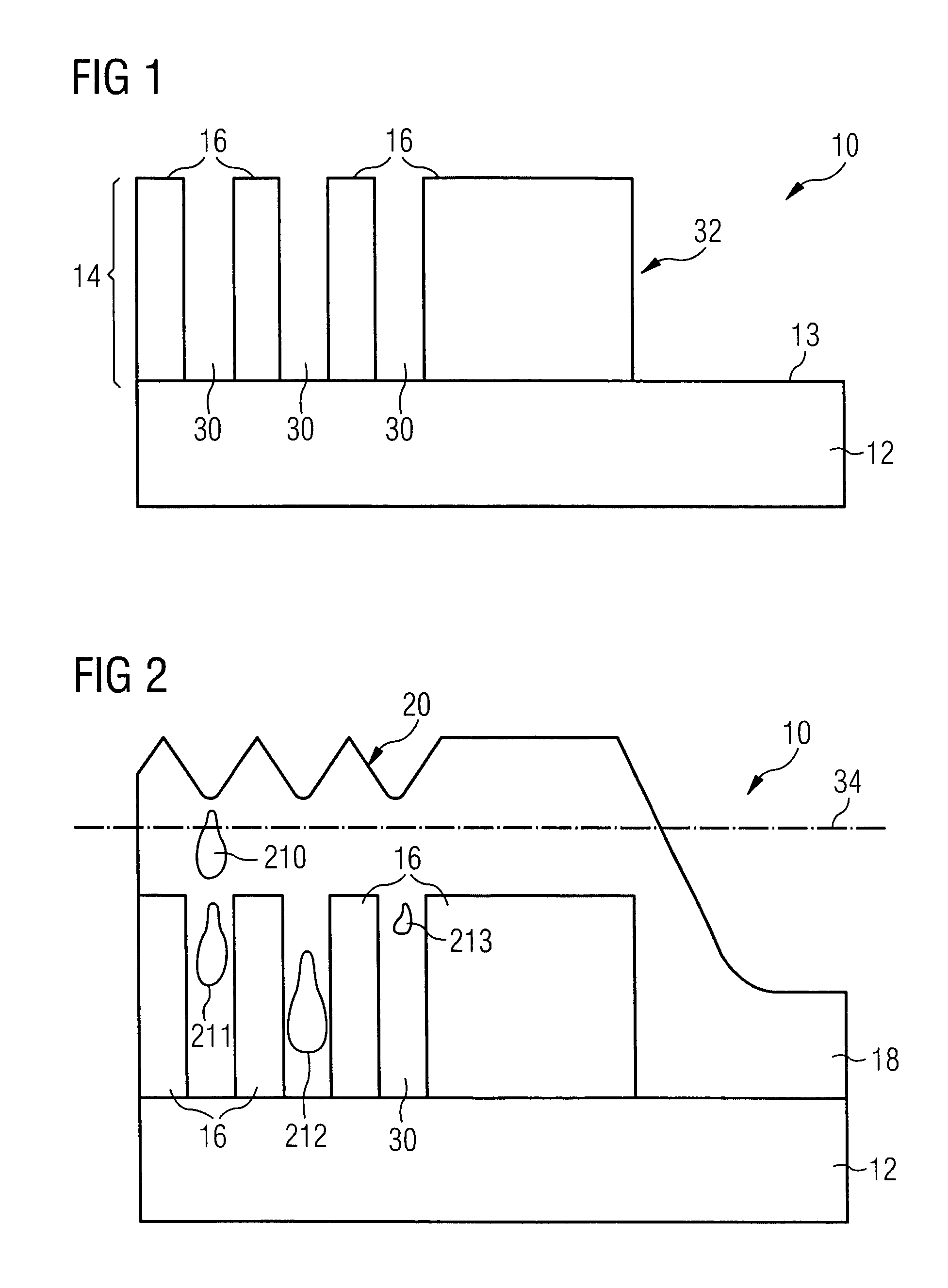
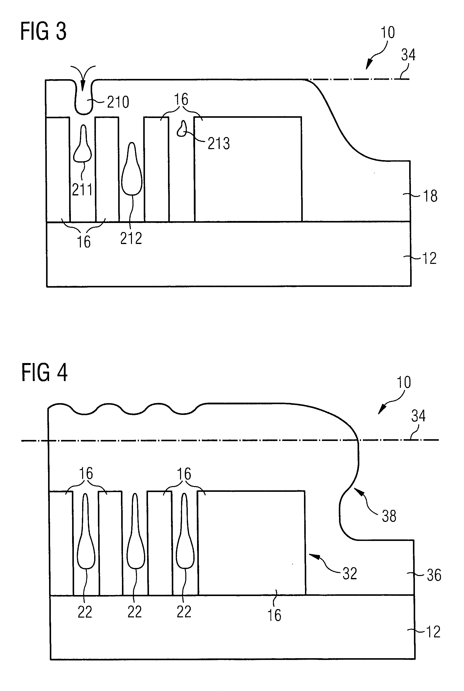
[0035]FIG. 1 shows a profile of raised structure elements arranged in parallel on a surface 13 of a semiconductor wafer 10. The raised structure elements are wiring lines 16, which correspond to a wiring level 14. Each two of the wiring lines 16 encompass spacings 30 formed in between the field of wiring lines. The outermost of the wiring lines 16 has an outer edge 32 oriented towards an area of the surface 13, which is not covered with wiring lines 16.

[0036] The surface 13 is provided by a planarized upper surface of an isolation layer 12, which pertains to a further wiring level arranged next below the present wiring level 14, and may contain a silicon oxide, a nitride, a doped silicon glass, etc. Alternatively, layer 12 may represent an isolation layer, which covers a silicon substrate (not shown).

[0037] The wiring lines 16 may comprise any electrically conductive material such as doped polysilicon or a metal, or a metal silicide, etc. It is further possible, that wiring lines ...


PUM


Abstract

A method of forming a wiring level and an electrical isolation associated with the wiring level on a surface of a semiconductor wafer comprises the steps of providing the semiconductor wafer having said surface, forming a plurality of electrically conductive wiring lines upon said surface, each of the wiring lines having a spacing with respect to neighboring one of the wiring lines, depositing a first layer of amorphous carbon upon the wiring lines by means of non-conformal plasma enhanced chemical vapor deposition (PECVD), such that air-filled voids formed below the first layer within the spacings between neighboring wiring lines. Alternatively, OSG (organo-silicon glass) or FSG (fluorine doped silicon glass) may be deposited to yield air-filled voids within the spacings. According to an embodiment, the carbon, OSG or FSG layers are used as an IMD-layer (line-to-line isolation), added by a further layer of a dielectric material, which then serves as an ILD-layer (level-to-level isolation).

Description

[0001] This application is a continuation-in-part of patent application serial number 11 / 246,916, entitled “Method of Forming an Electrical Isolation Associated with a Wiring Level on a Semiconductor Wafer,” filed on Oct. 7, 2005, which application is incorporated herein by reference.TECHNICAL FIELD [0002] The invention generally relates to manufacturing integrated circuits, and to manufacturing semiconductor wafers. In particular embodiments, the invention particularly relates to the formation of a wiring level and an electrical isolation associated with the wiring level on a semiconductor wafer. BACKGROUND [0003] In the field of manufacturing integrated circuits the process of forming conductive wiring levels, particularly metal levels, above a semiconductor substrate may be distinguished from the earlier formation of those electrical components, that depend on the presence of active areas within the monocrystalline silicon substrate. The corresponding process sequence aimed at th...

Claims


Application Information

Patent Timeline
IPC IPC(8): H01L21/4763
CPCH01L21/7682H01L23/5222H01L23/5329H01L23/53295H01L2924/0002H01L2924/00
Inventor OFFENBERG, DIRKVOGT, MIRKOSPERLICH, HANS-PETERCIGAL, JEAN CHARLES
Owner INFINEON TECH AG
Why Eureka
Try Eureka