
Solid state white light emitter and display using same

a light emitter and white light technology, applied in the direction of semiconductor devices for light sources, sustainable buildings, light and heating equipment, etc., can solve the problems of unreadable display, unsuitable replacement, and limited light output of leds,

Active Publication Date: 2005-03-10
KIRSTEEN MGMT GRP
View PDF15 Cites 91 Cited by
  • Summary
  • Abstract
  • Description
  • Claims
  • Application Information

AI Technical Summary

Benefits of technology

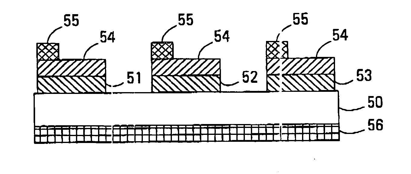
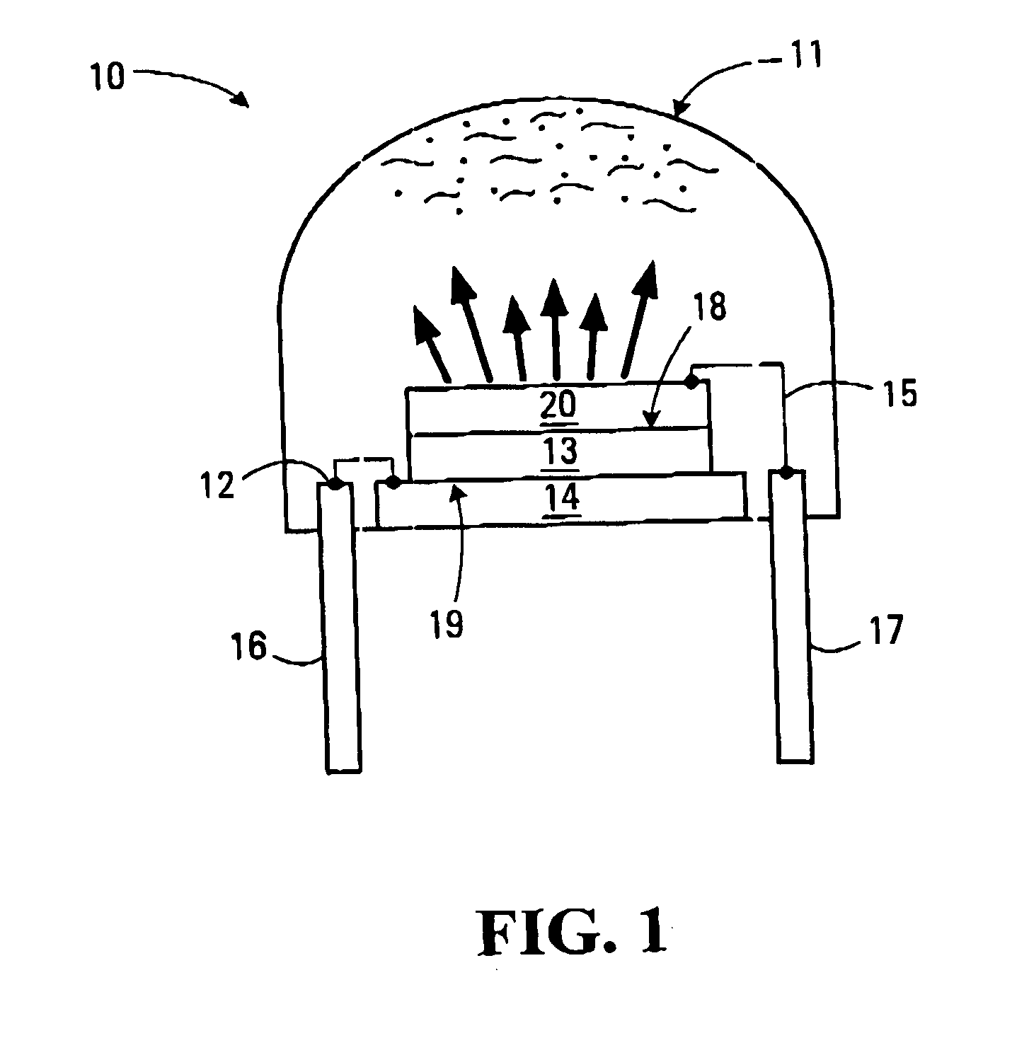
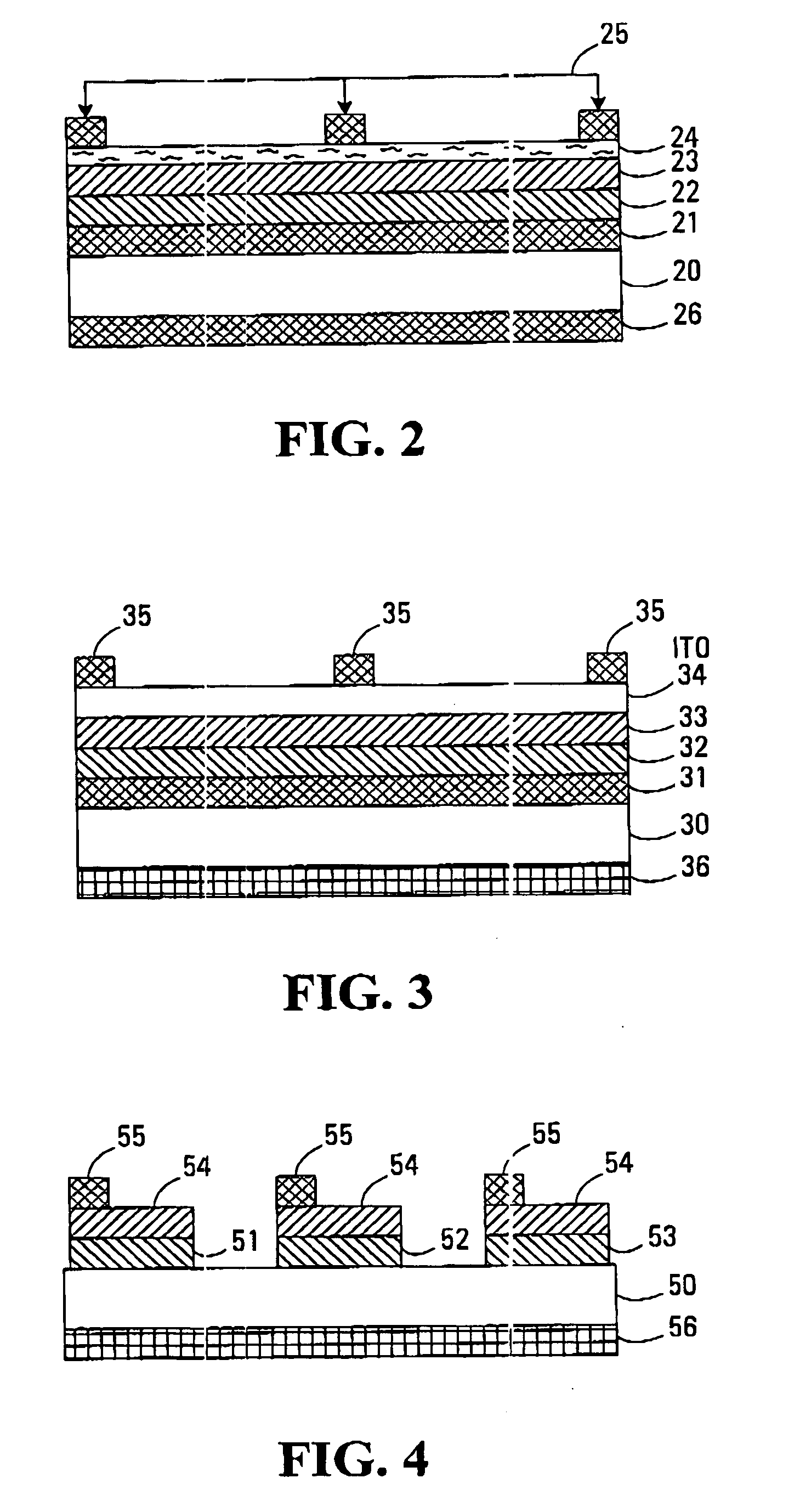
[0028] It is the purpose of some embodiments of the present invention to provide while light solid state luminescent devices using a single die, which use rare earth doped group IV semiconductor nanocrystals to generate the polychromatic white light, thus providing a solid state illumination device with white illuminance, without the need for multiple power leads or for more than one discrete LED lamp.
[0042] In some embodiments, the light emitting device further comprises a first electrode and a second transparent electrode across which a power supply signal can be applied to energize the light emitting device.

Problems solved by technology

Due to their long operation (burn) time and low power consumption, solid state light emitting devices frequently provide a functional cost benefit, even when their initial cost is greater than that of conventional lamps.
Until recently, LEDs have produced light only in the red, green or amber ranges and have not been generally suitable for replacing, for example, incandescent bulbs, with normally a white luminescence, in a wide variety of display applications.
Such recurrent failures make a display unreadable and, therefore, not useful.
These conditions (i.e., broken or missing pixels) require constant repair leading to a significant maintenance problem for providers of display signs based on incandescent illumination devices.
Due to severe environmental conditions on roadways, glass breakage of incandescent and fluorescent lamps is an all too frequent mishap.
Thus the maintenance costs related to replacement of non-operational incandescent lamps or miniature fluorescent (or neon) lamps are high and unfortunately, continual.
Given the desirability of white light displays (e.g., commercial bank “time and temperature” message boards, stadium scoreboards), considerable effort has been expended to produce white light LEDs.
The multiple LEDs would be then incorporated into complicated and expensive LED modules to obtain the required broad band illumination necessary to provide white light.
These complicated multiple die, variable color devices provide an expensive and complicated method of offering white light illumination.
Furthermore, these multiple die white lamps are rather inefficient in the present state of the art, offering luminosity far below that realized by existing monochromatic light emitting diode lamps, even when a very large quantity of dies are functionally incorporated into the discrete lamp assembly.
However, at present there is a very limited number c)f such solid state lamps available.
However, the methods of fabricating white LED lamps are limited.
While the lamps that make up the modules may be individually addressable, and hence, offer the opportunity to, selectively and individually, provide red, green and blue light (or combinations thereof), such modular systems are complex and costly means of providing white light for a solid state display.
Thus, this multiple die LED lamp would be rather expensive to fabricate, and would require expensive and complicated circuitry to power and control in an outdoor display.
However, these light emitting devices are not solid-state, and miniaturization of these fluorescent bulbs to provide suitable pixel resolution for display applications has never been practically accomplished.
In fact:, the primary application of miniature fluorescent lamps (with long operational lifetimes, but unfortunately high power consumption when compared with solid state LED lamps) in displays is to provide back lighting to liquid crystals that are individually addressed at the pixel level.
Furthermore, these miniature fluorescent lamps remain fragile light emitting devices by virtue of their glass housings and are unsuitable for use in display applications in which the lamps are exposed to extreme environmental stresses.
Such stresses can not only break the glass housing, but effect delamination of the powder coatings from the interior wall of the glass housing.
While it is useful for a single device to be constructed in which dopants offer a multitude of luminescent wavelengths, dopants invariably alter the electrical and lattice structures of semiconductors and as such, the performance of these devices are considerably poorer than for corresponding semiconductors free of dopant that emit monochromatic irradiation, as a result of being dopant-free.
While organic materials have been utilized to prepare certain thin-film electroluminescent devices, no organic based LEDs are commercially available.
Further, organic-based LEDs are at present plagued by extremely short operational lifetimes due to degradation of the organic charge-transfer materials.
Not withstanding the progress made in using organic fluorescers as luminescent sites within either electron-transport or hole-transport layers and affording thin-film interfacial hole-electron recombination, the current state of the art finds it difficult to generate organic based dies with reasonable operational lifetimes. By their very nature, these donor-acceptor complexes are prone to reaction with the surrounding medium.
As a result, many of these organic molecules degrade under constant excitation to the excited state and consequently the organic-based LEDs fail.
Those fluorescers with extremely high quantum, yields of fluorescence, which by definition necessitate short excited state lifetimes and are unlikely to be quenched or degraded by oxygen or other reactants, do not have sufficient electron or hole transport properties to allow for device-wide localized hole-electron recombination in the ground state.

Method used


Image

  • Solid state white light emitter and display using same
  • Solid state white light emitter and display using same
  • Solid state white light emitter and display using same

Examples


example 1

[0189] Silane (SiH4) and Oxygen (O2) are added to an argon plasma stream produced by an Electron Cyclotron Resonated (ECR) reactor via dispersion ring. The ratio (Q) of silane to oxygen has been varied between 3:1,1.7:1,1.2:1,1:1.9, and 1:2. An erbium precursor (Tris(2,2,6,6-tetramethyl-3,5-heptanedionato) erbium(III) [Er+3(TBMD)3]) is placed in a stainless steel oven held between 90 and 110° C.

[0190] A carrier gas of Ar is used too transport the Er precursor from the oven through a precision controlled mass-flow controller to a dispersion ring bellow the Silane injector and above the heated substrate. The instrument pressure is kept at about 1×10⁻⁷ torr. The substrates used are either fuse silica or silicon wafers on which is thermally grown an oxide layer of 2000 nm thickness. The deposition temperature, the microwave power and the sceptre bias are kept constant at 300° C., 400W and −200Vdc. The SiH4, Ar flow rates were adjusted while keeping the O2 flow rate at 20 militori sec−1...

example 2

[0191] An ablation target is fabricated by combining powdered silicon, powdered silicon dioxide and powdered erbium oxide, the prepared powder mixture comprising 45% silicon, 35% silicon oxide and 20% erbium oxide. Each powder component has a size of about 300 mesh. The mixture is placed into a ball mill and ground for approximately 5 to 10 minutes. The mixture is then placed into a 25 mm diameter by 7 mm thick mould, placed into a hydraulic press, and compressed for 15 minutes at 500 psi. The obtained target is then placed into an annealing furnace and heated to 1200° C. in a forming gas atmosphere of 5% H2 and 95% N2 for 30 minutes. The Target is cooled down to room temperature and then reground in a ball mill for ten minutes. The mixture is then again placed in a mould, compressed and annealed as described above. The obtained target is placed onto a target holder inside a vacuum chamber. A silicon substrate [n-type, single crystal, 0.1-0.5 Ωcm conductivity] of 50 mm diameter and...

example 3

[0193] A gas pyrolysis apparatus was; fitted with a small tubular furnace having a length of 3 cm and an interior diameter of 12 mm. While the furnace temperature was held between 900 and 950° C., an argon carrier gas, silane (SiH4), and Er+3(THMD)3 were introduced to the furnace by way of precision mass-flow controllers. The Er+3 (THM)3 was transferred to the gaseous phase through the use of a temperature controlled oven. The flow through the apparatus was assisted by a mechanical vacuum pump at the end of the apparatus. Once through the furnace, the gaseous stream was allowed to pass through a cooling zone and then to pass through a two-stage bubbler of ethylene glycol. The ethylene glycol solution was removed from the bubbler and it was vacuum dried to cover Er doped Si nanocrystals having an average diameter of about 3 nm.


PUM

PropertyMeasurementUnit
thicknessaaaaaaaaaa
grain sizeaaaaaaaaaa

Abstract

A light emitting assembly comprising a solid state device coupleable with a power supply constructed and arranged to power the solid state device to emit from the solid state device. A series of rare-earth doped silicon and / or silicon carbide nanocrystals that are either combined in a single layer or in individual layers that produce the required Red, Green, and Blue (RGB) emission to form a white light.

Description

RELATED APPLICATIONS [0001] This application claims the benefit of U.S. Provisional Application No. 60 / 500,686 filed Sep. 8, 2003.FIELD OF THE INVENTION [0002] This invention relates to solid state light emitting devices and more particularly to such devices which produce white light. BACKGROUND OF THE INVENTION [0003] Solid state light emitting devices such as light emitting diodes are extremely useful because they potentially offer lower fabrication costs and long term durability benefits over conventional incandescent and fluorescent lamps. Due to their long operation (burn) time and low power consumption, solid state light emitting devices frequently provide a functional cost benefit, even when their initial cost is greater than that of conventional lamps. However, because large scale semiconductor manufacturing techniques can be used, many solid state lamps can be produced at extremely low cost. One such device is the solid state light emitting diode (LED) which has low fabrica...

Claims


Application Information

Patent Timeline
Patent Type & Authority Applications(United States)
IPC IPC(8): C09K11/77F21K99/00H01L29/04H01L33/18
CPCB82Y20/00C09K11/77Y02B20/181H01L33/18F21K9/00Y02B20/00
Inventor HILL, STEVEN E.
Owner KIRSTEEN MGMT GRP
Learn More