Organic electroluminescent device
- Summary
- Abstract
- Description
- Claims
- Application Information
AI Technical Summary
Benefits of technology
Problems solved by technology
Method used
Image

Examples
first embodiment
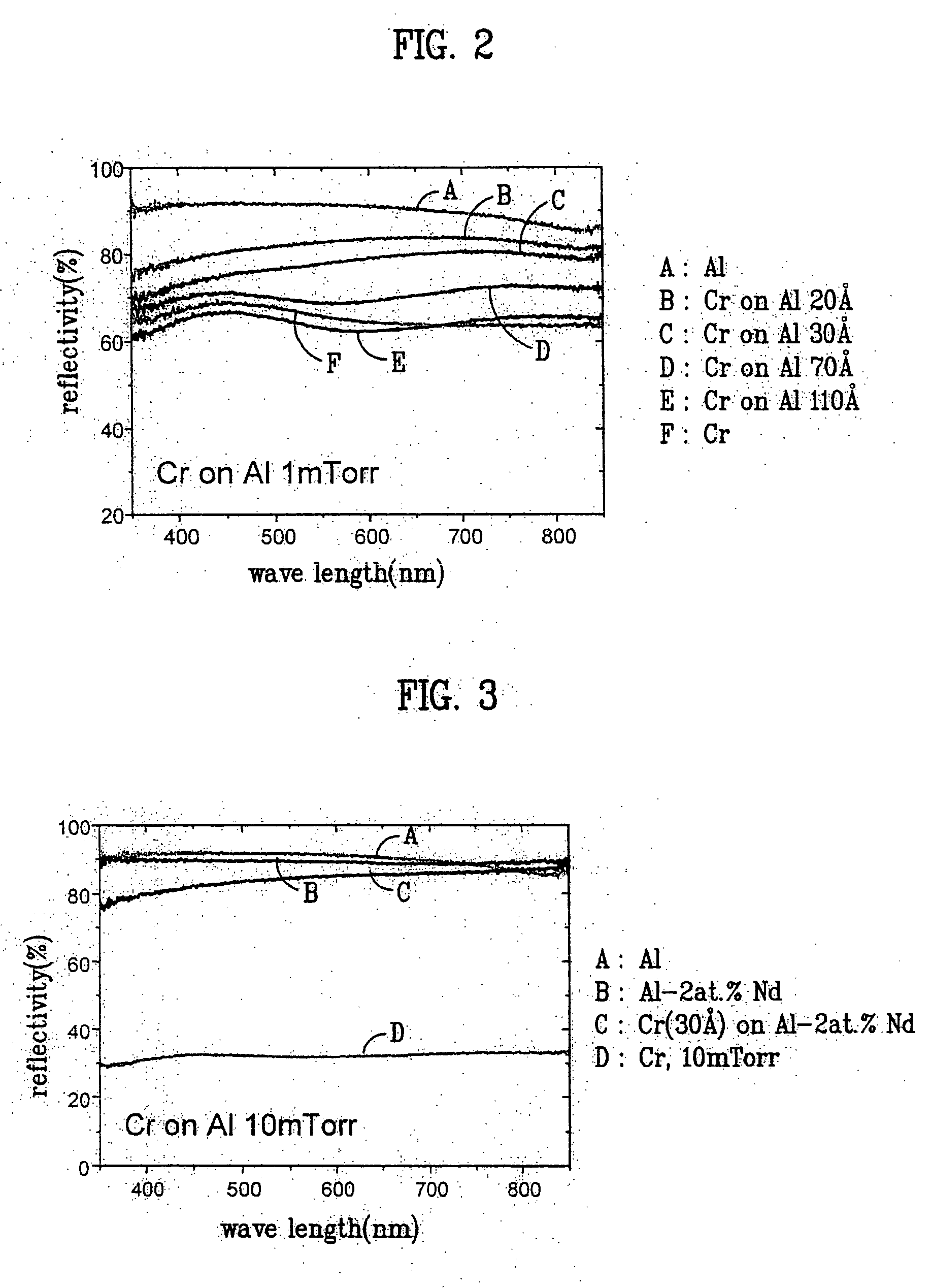
[0052]FIG. 2 is a graph of reflectivity variation depending on thickness of Cr layer on Al layer according to the present invention.
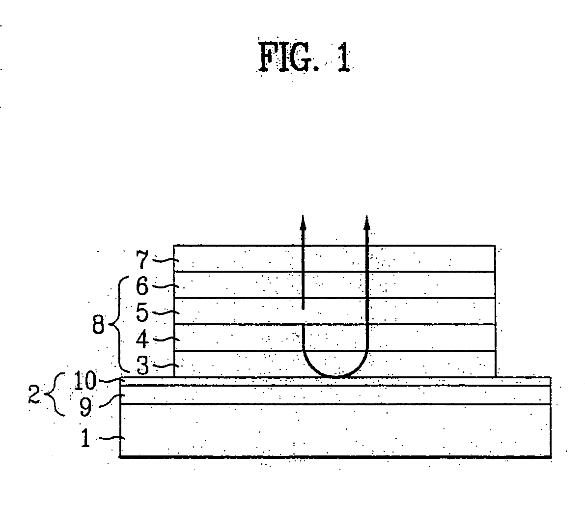
[0053] Referring to FIG. 2, the anode 2 includes the reflective layer 9 of Al and the hole injection layer 10 of Cr.
[0054] Al layer is deposited 150 nm thick using 4″ target of 99.999% at 200 W and 2 mTorr. Cr layers are deposited 2 nm, 3 nm, 7 nm, and 11 nm thick, respectively using 4″ target of 99.999% at 200 W and 1 mTorr.
[0055] As shown in the drawing, the more the thickness of Cr increases, the more overall reflectivity of the anode 2 decreases.
[0056] In case that the thickness of Cr exceeds 1 nm, the corresponding reflectivity is lower than reflectivity of the single Cr layer. Hence, it is unable to achieve the object of the present invention in improving the reflectivity.
[0057] By providing Cr with the thickness less than 10 nm, the reflectivity can be improved.
[0058] In doing so, if the deposition condition of Cr is varied to 10 mTorr, the ...
second embodiment
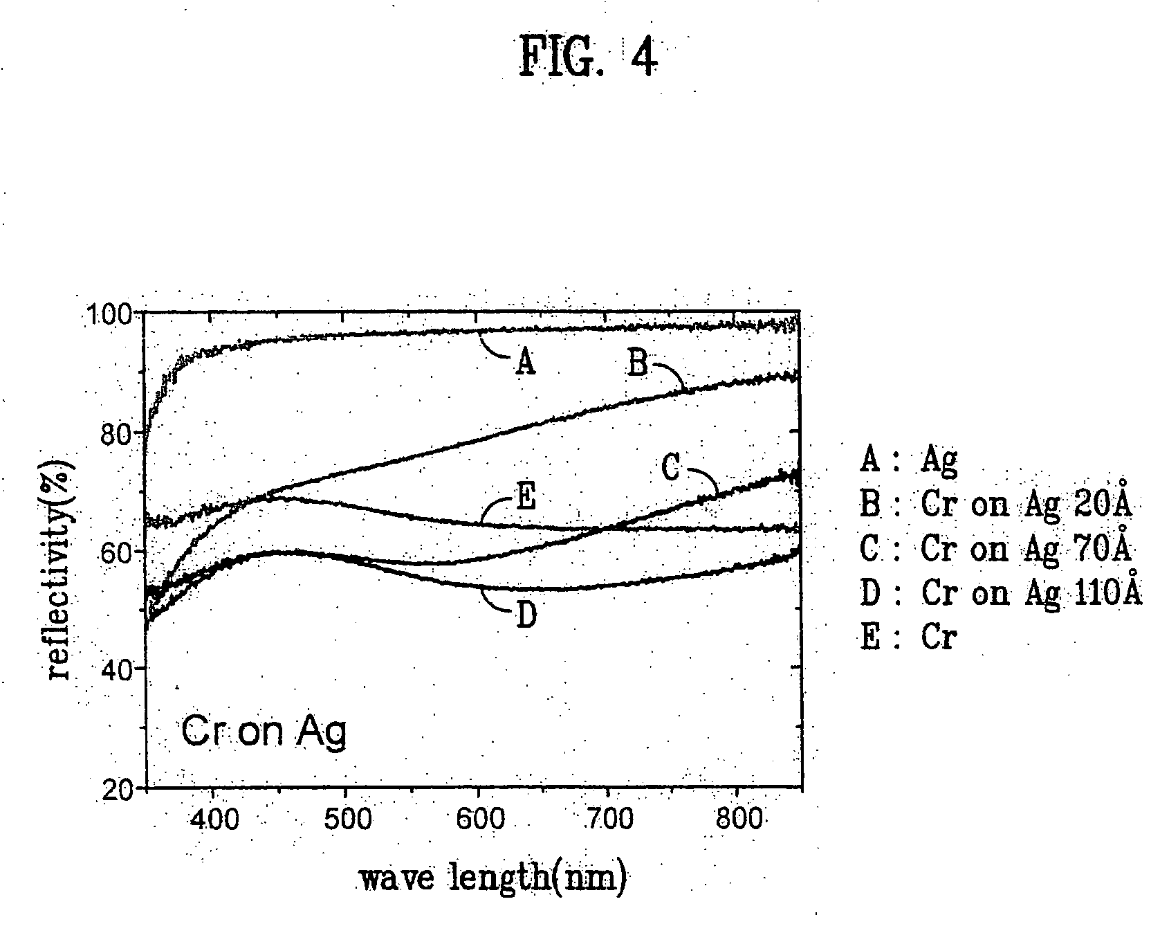
[0060]FIG. 3 is a graph of reflectivity variation depending on thickness of Cr layer on Al—Nd alloy reflective layer according to the present invention.
[0061] Referring to FIG. 3, instead of the Al layer, the reflective layer 9 for the anode 2 is formed 150 nm thick using 4″ Al-2 at. % Nd alloy target of 99.999% at 200 W and 1 mTorr.
[0062] And, a Cr layer as the hole injection layer 10 is formed 3 nm thick on the reflective layer 9 using 4″ target of 99.999% at 200 W and 10 mTorr.
[0063] Compared to the reflectivity of the case of the mono-atomic Al layer, reflectivity in the visible ray area is reduced about 2% in case of using the 2 at. % Nd-added Al target.
[0064] Yet, even if the Cr layer is deposited on the Al—Nd layer, it can be checked that there is almost no variation of the reflectivity of the Al—Nd layer.
[0065] Thus, if the alloy formed by adding one of Nd, Ta, Nb, Mo, W, Ti, Si, B, and Ni at about 5 at. % to Al is used as the reflective layer 9, reduction of the reflect...
PUM
| Property | Measurement | Unit |
|---|---|---|
| Thickness | aaaaa | aaaaa |
| Thickness | aaaaa | aaaaa |
| Electrical resistance | aaaaa | aaaaa |
Abstract
Description
Claims
Application Information
 - Generate Ideas
- Intellectual Property
- Life Sciences
- Materials
- Tech Scout
- Unparalleled Data Quality
- Higher Quality Content
- 60% Fewer Hallucinations
Browse by: Latest US Patents, China's latest patents, Technical Efficacy Thesaurus, Application Domain, Technology Topic, Popular Technical Reports.
© 2025 PatSnap. All rights reserved.Legal|Privacy policy|Modern Slavery Act Transparency Statement|Sitemap|About US| Contact US: help@patsnap.com