Novel photonic waveguide structures for chip-scale photonic integrated circuits

a photonic integrated circuit and chip-scale technology, applied in the field of micro and nanophotonic waveguide fabrication, can solve the problems of inability to fabricate devices using waveguides produced by these methods, and inability to meet the requirements of refractive index differential, etc., to achieve the effect of simple refractive index differential requirements, low cost and light weigh

Inactive Publication Date: 2005-01-06
APPLIED RES & PHOTONICS
View PDF12 Cites 30 Cited by
  • Summary
  • Abstract
  • Description
  • Claims
  • Application Information

AI Technical Summary

Benefits of technology

[0029] In this disclosure a new class of photonic waveguide is described that are based on the natural index contrast (NIC) principle. This method simplifies the refractive index differential requirements between the core and the cladding of waveguide. The NIC based waveguide forms the basis of a class of chip-scale photonic integrated circuit where different functionalities are fabricated on a single chip and are connected via on-chip waveguide interconnects. This new waveguide technology enables development of low cost, light weight, nanophotonic systems by utilizing the NIC effect of dendrimer, nano silica, spin-on glass, other nano-materials and compositions of the said materials. Further, a number of photonic integrated circuits (PICs) can be designed based on the NIC based waveguides for optical signal processing and optical amplification, optical modulation, and wavelength routing.
[0034] The present invention discloses an alternative method where built-in refractive index difference of compatible materials is used to form the waveguide core and cladding, thus avoiding direct doping of glasses. This method, called the natural index contrast (NIC) method is an attractive alternative for photonic waveguide design. Here the materials are matched to form the core and the cladding utilizing the built-in index contrast. This eases a big hurdle of controlling the RI via doping methods. The NIC method offers a straightforward solution to produce a step index profile with the possibility to expand to graded index profile as well, while fabrication is significantly simpler than contemporary methods. Since the PICs are based on step index waveguides, NIC method is suitable for a number of PIC based devices. The concept is applicable to any photonic waveguide design where the built-in refractive index contrast is suitable for waveguiding from a chosen set of material. The present invention focuses on waveguides suitable for guiding light in the range of 1060 nm and 1600 nm.
[0036] What distinguishes dendrimers from other materials is the fact that it offers properties similar to dielectric materials in a polymeric form. Dendrimers are a novel class of three-dimensional nanoscale, core-shell molecules that can be precisely synthesized for a wide range of applications. Building on a central core molecule, dendrimer molecules are formed by the step-wise, sequential addition of concentric shells consisting of branched molecules and connector groups. Each branched shell is referred to as a generation. Up to ten generations can be incorporated into a single dendrimer molecule, thus allowing a wide range control of the size and number of functional groups of each molecule. Some important properties of this class of polymers can be found at the DNT web at http: / / dnanotech.com / properties.html.
[0045] At the second phase of integration, appropriate on-chip gain elements (e.g., Er3+ doped waveguide amplifier) can be combined with these chips to produce the above mentioned PICs with low-loss and / or with a gain. This is important, because, optical transmission systems require frequent signal amplification and regeneration (also called repeater) that is expensive and adds complexity to system design. Ability to build systems with extremely low-loss and / or gain will simplify system design significantly. It will also eliminate the frequent need of signal regeneration, thus enabling significant cost savings and ease of deployment of fiberoptic systems.
[0048] The objective of a chip-scale PIC is to produce a very concise device with multiple functionalities on a single substrate. Two different schemes are usually considered: (i) system-on-chip, and (ii) chip-scale packaging; both of these schemes actually complement each other. The triple-phase integration scheme, as described above, allows a PIC (e.g., a RAWG) to be further integrated over several phases to produce denser functionality on the same substrate. For instance, a RAWG monolithically attached with amplifying waveguide blocks allows controlling the loss factor. Further, lasers and modulators can be added to the RAWG to produce multichannel transmitters. One can then add detectors to add more functionality enabling transceivers, transponders, and switching on a chip as well. Finally, combined with CMOS processes, these PICs can be used to build self containing optical communication router. However, here we emphasize on monolithic integration, as opposed to hybrid integration where different elements are packaged together on a single substrate or in a single box.

Problems solved by technology

Present methods of fabrication of photonic waveguide (also referred to as planar waveguide in the literature) are complicated.
These methods are inherently complicated and devices produced from the waveguides fabricated by these methods are performance limited.
Because the precursor is delivered in the form of gas, and the proportion of dopant precursor determines the concentration of dopant in glass, it is difficult to control the processing factors.
As a result, the refractive index may suffer from non-uniformity across the thickness of the deposited layer; hence, a sharp boundary between the glass-layers of two different refractive indexes is difficult to obtain, causing a poor quality of the waveguides.
However, ion exchange method suffer from limitations that it cannot precisely control the dimensions of the waveguide and does not form a sharp demarcation line between the refractive indices of the core and the cladding.
This is more problematic in case of solution phase diffusion of ions into the substrate because the ions can diffuse in all directions.
Due to these problems, the ion exchange method is not efficient to control the waveguide properties with a sharp step refractive index between the core and the cladding.
In general, existing methods of producing photonic waveguides suffer from performance limitation and ease of fabrication.
Moreover, these methods require expensive and dedicated machineries that are not easily amenable to different materials system and / or processes.

Method used


Image

  • Novel photonic waveguide structures for chip-scale photonic integrated circuits
  • Novel photonic waveguide structures for chip-scale photonic integrated circuits
  • Novel photonic waveguide structures for chip-scale photonic integrated circuits

Examples


Embodiment Construction

[0031] Natural Index Contrast Effects

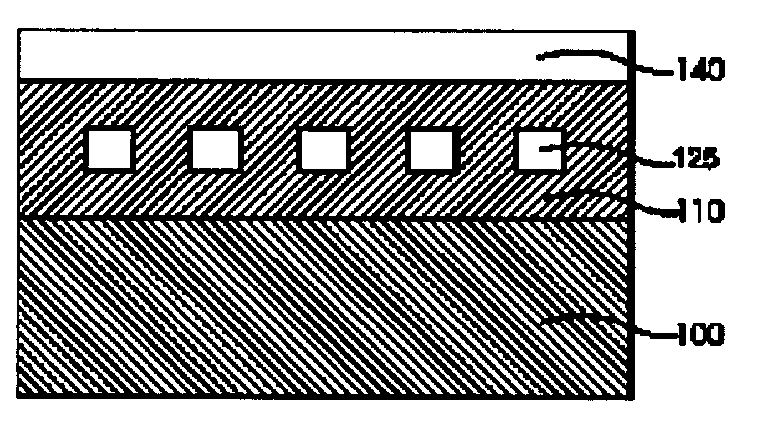
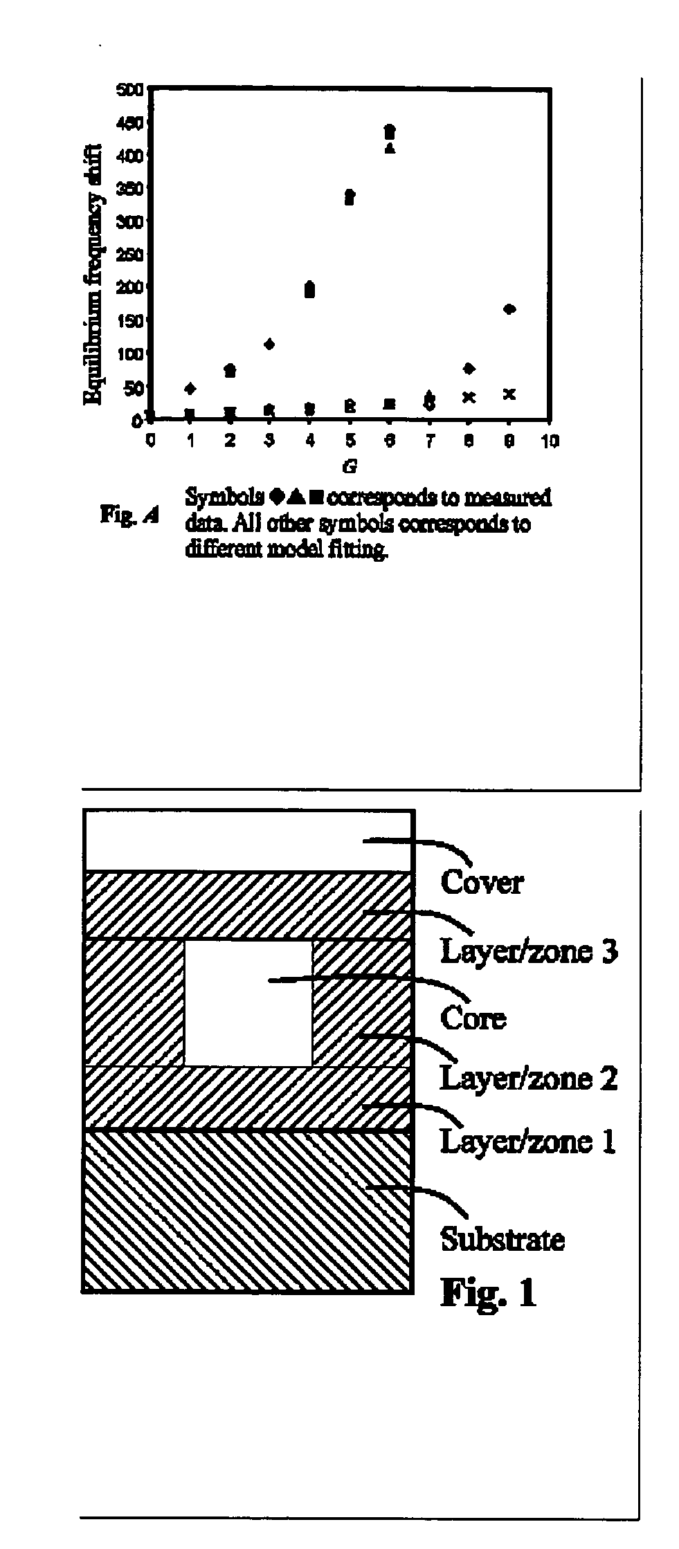
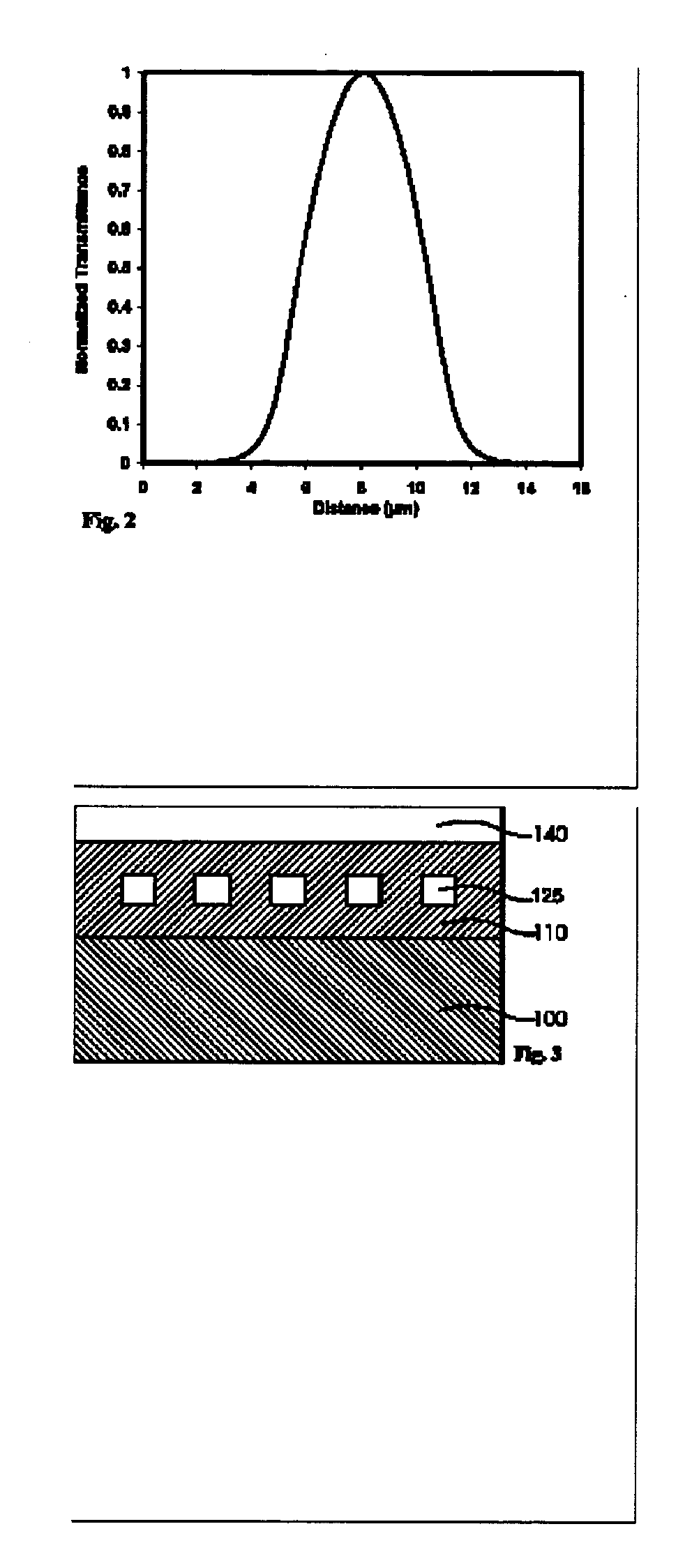
[0032] When two layers of two different materials are brought in contact of each other at an interface, there exists an energy difference similar to the energy levels produced in a semiconductor by dopant atoms. In case of dielectric thin films of two different materials, one laid on top of another, there will be a difference in refractive index (RI) between the two layers. Light, incident at an appropriate angle on these layers, will bend towards the higher RI material at the interface (the total internal reflection). When a higher RI material is completely enclosed in a lower RI material, incident light will propagate within the enclosed region thus forming a waveguide, similar to a step index optical fiber. The guiding layer is called the core and the surrounding layer is called the cladding.

[0033] Existing methods for fabricating waveguides are mostly based on glass based materials where expensive equipments are necessary for deposition, do...


PUM


Abstract

The present invention discloses a concept of natural index contrast (NIC) for producing photonic waveguides and methods of fabrication thereof. Such waveguide forms the basis of a class of chip-scale micro- and nano-photonic integrated circuits (PICs). The NIC method utilizes the built-in refractive index difference between two layers of dielectric thin films of two different materials, one laid on top of another. This new class of waveguides simplifies the PIC fabrication process significantly. Based on the NIC based waveguides, PICs can be fabricated for a number of photonic applications such as arrayed waveguide grating (AWG), reflective arrayed waveguide grating (RAWG), interleaver, interferometer, and optical sensor. Additionally, several other PICs can also be fabricated via tiers of integration, such as triple-phase integration. Examples of such devices include optical amplifier, wavelength router, sensor, optical modulator, transmitter, receiver, transponder, fully built dense wavelength division multiplexer and demultiplxer, optical power splitter, multicahnnel tunable optical attenuator, and multicahnnel tunable optical add-drop multiplexer. Unlike hybrid integration, triple-phase integration monolithically integrates multiple optical functionalities on a single chip.

Description

CROSS REFERENCE [0001] U.S. Pat. No. 0,024,274A1 (Feb. 6, 2003) titled “Method of manufacturing a planar waveguide using ion exchange method.”[0002] K. Okamoto “Fundamentals of Optical Waveguides, Ch. 9”, Academic Press, New York, 2000. [0003] K. M. A. Rahman, C. J. Durning, N. J. Turro and D. A. Tomalia, “Adsorption of Poly(amido amine) Dendrimers on Gold,” Langmuir2000, 16, 10154-10160. [0004] K. M. Anis Rahman, Christopher J. Durning and Nicholas J. Turro, “Molecular Dynamics of PAMAM Dendrimers,” http: / / dwdm2.home.comcast.net / pamamdynamics.pdf. [0005] DNT web at http: / / dnanotech.com / properties.html. [0006] A. Otomo, S. Otomo, S. Yokoyama, T. Nakahama, and S. Mashiko, “Remarkable optical properties of dendrimers for laser applications,” in Linear and nonlinear optics of organic materials, Eds. M. Eich and M. G. Kuzyk, Proceedings of SPIE vol.4461, 180-187, 2001. [0007] A. K. Y. Jen, H. Ma, T. Sassa, S. Liu, S. Suresh, L. R. Dalton, and M. Hailer, “Highly efficient and thermally s...

Claims


Application Information

Patent Timeline
IPC IPC(8): G02B6/122
CPCG02B6/1221B82Y30/00
Inventor RAHMAN, ANISTOMALIA, DONALD
Owner APPLIED RES & PHOTONICS
Why Eureka
Try Eureka