Amorphous diamond materials and associated methods for the use and manufacture thereof
a technology of diamond materials and diamonds, applied in the manufacture of discharge tubes/lamps, discharge tube main electrodes, electrode systems, etc., can solve the problems of limiting the potential and limiting the use of field emission devices. , the effect of reducing the number of defects
- Summary
- Abstract
- Description
- Claims
- Application Information
AI Technical Summary
Benefits of technology
Problems solved by technology
Method used
Image
Examples
example 2
[0075] A 10 micron layer of copper can be deposited on a substrate using sputtering. Onto the copper was deposited 2 microns of samarium by sputtering onto the copper surface under vacuum. Of course, care should be taken so as to not expose the beryllium to oxidizing atmosphere (e.g. the entire process can be performed under a vacuum). A layer of amorphous diamond material can then be deposited using the cathodic arc technique as in Example 1 resulting in a thickness of about 0.5 microns. Onto the growth surface of the amorphous diamond a layer of magnesium can be deposited by sputtering, resulting in a thickness of about 10 microns. Finally a 10 microns thick layer of copper was deposited by sputtering to form the anode.
example 3
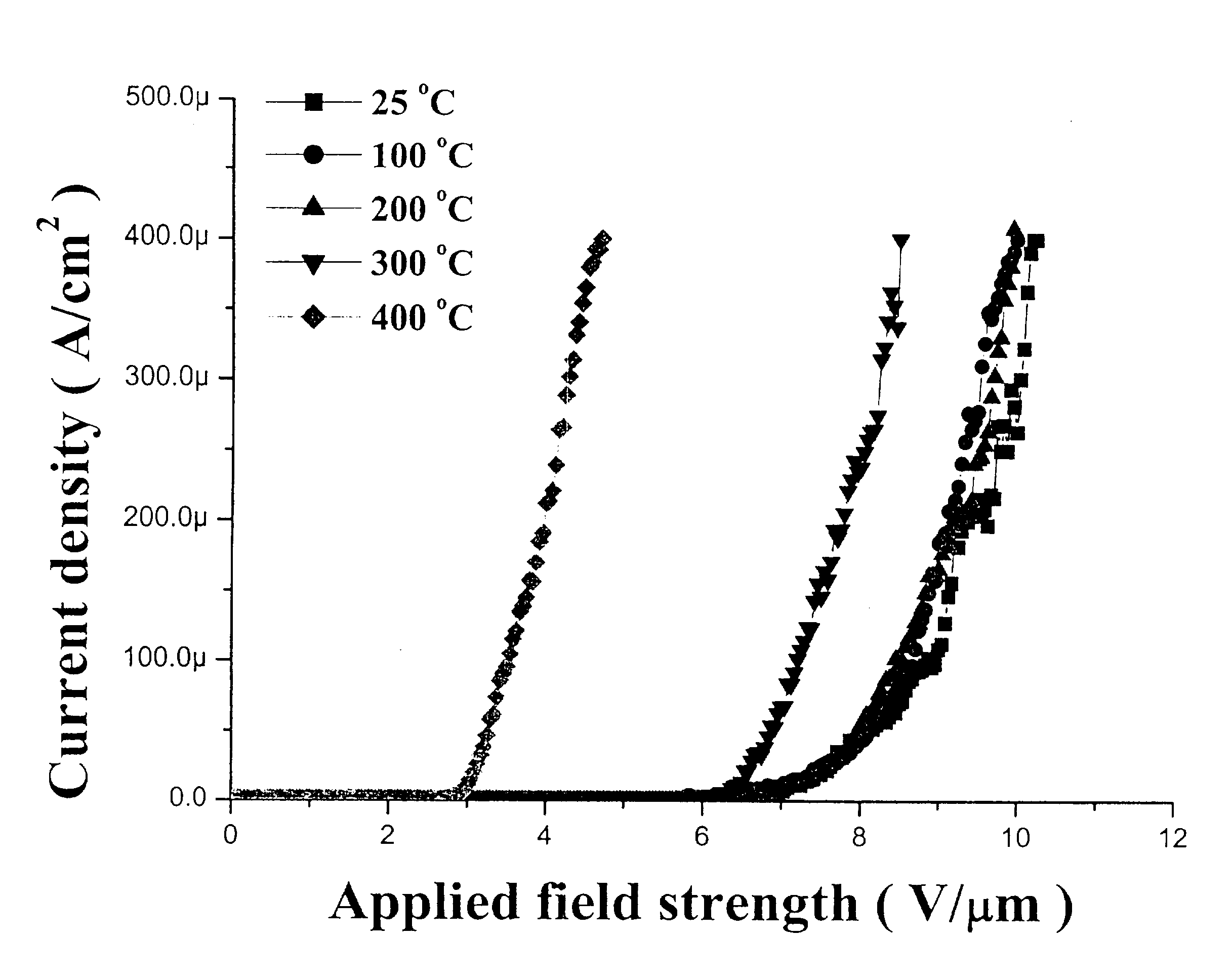
[0076] A 10 micron layer of copper can be deposited on a substrate using sputtering. Onto the copper was deposited 2 microns of cesium by sputtering onto the copper surface under vacuum. Of course, care should be taken so as to not expose the cesium to oxidizing atmosphere (e.g. the entire process can be performed under a vacuum). A layer of amorphous diamond material can then be deposited using the cathodic arc technique as in Example 1 resulting in a thickness of about 65 nm. Onto the growth surface of the amorphous diamond a layer of molybdenum can be deposited by sputtering, resulting in a thickness of about 16 nm. Additionally, a 20 nm thick layer of In--Sn oxide was deposited by sputtering to form the anode. Finally, a 10 micron layer of copper was deposited on the In--Sn layer by sputtering. The cross-sectional composition of the assembled layers is shown in part by FIG. 9A as deposited. The assembled layers were then heated to 400.degree. C. in a vacuum furnace. The cross-se...
PUM
| Property | Measurement | Unit |
|---|---|---|
| height | aaaaa | aaaaa |
| work function | aaaaa | aaaaa |
| thickness | aaaaa | aaaaa |
Abstract
Description
Claims
Application Information
 - R&D
- Intellectual Property
- Life Sciences
- Materials
- Tech Scout
- Unparalleled Data Quality
- Higher Quality Content
- 60% Fewer Hallucinations
Browse by: Latest US Patents, China's latest patents, Technical Efficacy Thesaurus, Application Domain, Technology Topic, Popular Technical Reports.
© 2025 PatSnap. All rights reserved.Legal|Privacy policy|Modern Slavery Act Transparency Statement|Sitemap|About US| Contact US: help@patsnap.com


