Separation-material composition for photo-resist and manufacturing method of semiconductor device
a technology of separation material and semiconductor device, which is applied in the direction of photosensitive material processing, photomechanical equipment, instruments, etc., can solve the problems of high resistance value between the upper and lower wiring patterns, deterioration of operation speed, and increase of power consumption
- Summary
- Abstract
- Description
- Claims
- Application Information
AI Technical Summary
Benefits of technology
Problems solved by technology
Method used
Image
Examples
embodiment 2
[0211] This modified example is a modified example of the exemplified practical embodiment 2 and at the same time is one example of a practical embodiment according to the first invented method.
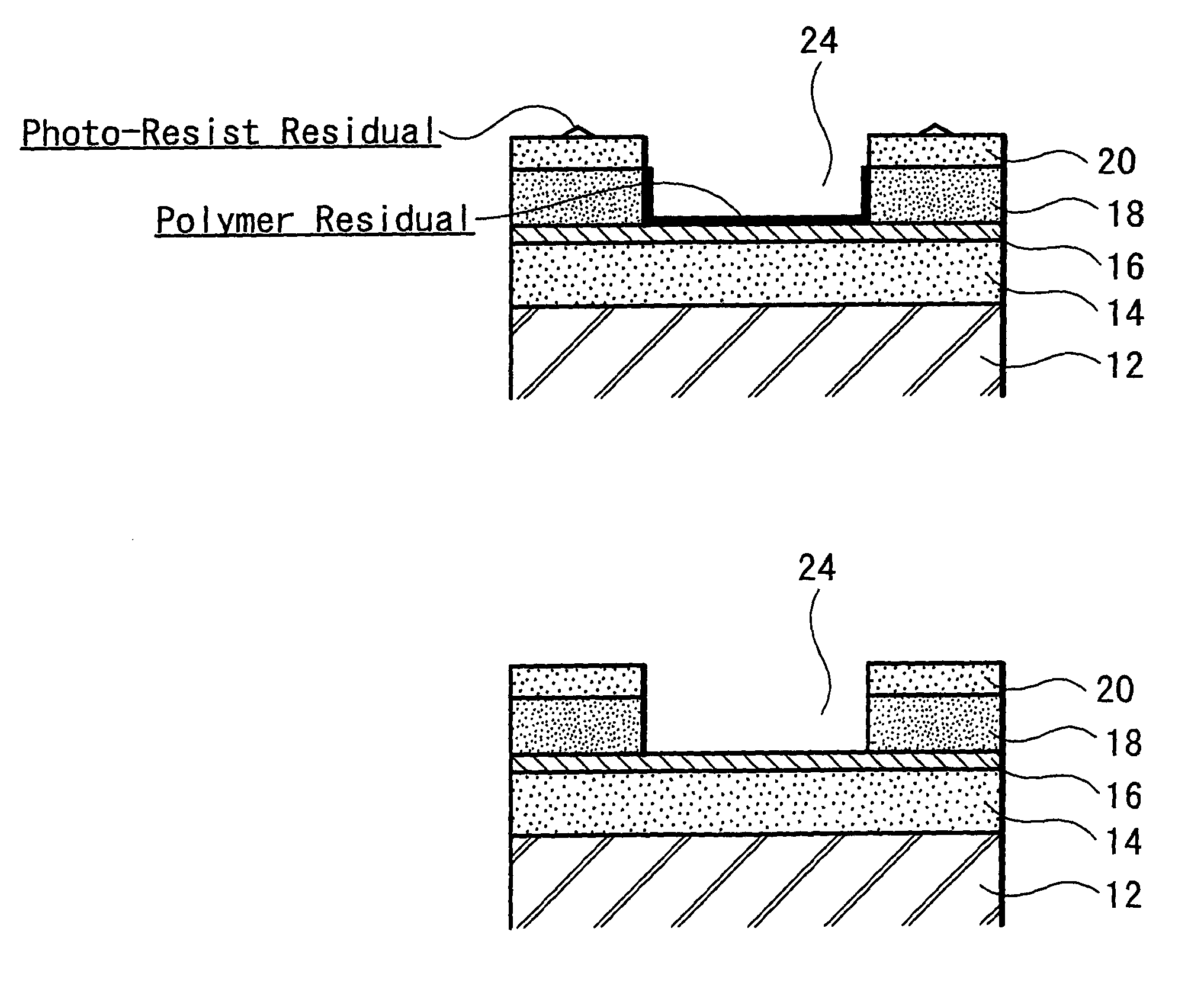
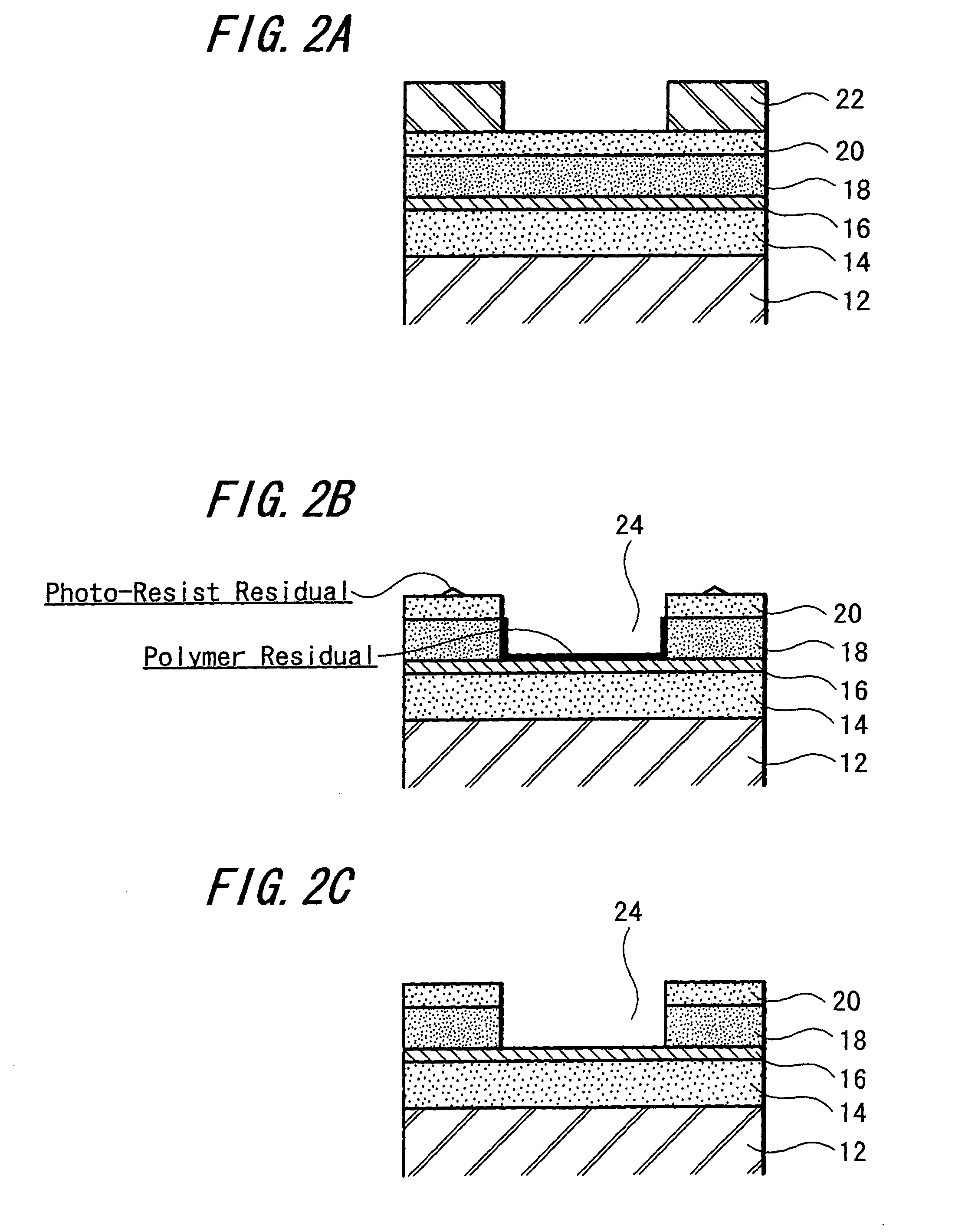
[0212] In this modified example, as shown in FIG. 4B, the reflection prohibition film 44, the cap insulation film 42, the low dielectric-constant insulation film 40, the etching-stopper layer 38 and the low dielectric-constant insulation film 36 are etching processed from the upper side of the photo-resist mask 45, the etching process is stopped at the surface of the etching-stopper layer 34, the wiring groove 46 is formed, and thereafter when the photo-resist mask 45 is removed, the photo-resist mask 45 and reflection prohibition film 44 are separated by a medicinal liquid washing process using the separation-material composition for the photo-resist of the exemplified practical embodiment 2 for 15 minutes instead of an ashing process. Subsequently, a pure water rinsing process and a drying ...
embodiment 3
[0220] An Exemplified Practical Embodiment 3 of a Manufacturing Method of a Semiconductor Device:
[0221] This exemplified practical embodiment is still another example of a practical embodiment of a manufacturing method of a semiconductor device with reference to the second invented method, and FIGS. 8A to 8D are cross-sectional views of processes respectively when a wiring structure of a single layer is formed according to this exemplified practical embodiment.
[0222] This exemplified practical embodiment is an example of forming a wiring structure of a single layer on the base substrate and first, as shown in FIG. 8A, a first wiring 74 which is constituted by a Ti film 74a of a film thickness 20 nm, a TiN film 74b of a film thickness 20 nm, an Al-0.5% Cu film 74c of a film thickness 500 nm, a Ti film 74d of a film thickness 5 nm and a TiN film 74e of a film thickness 100 nm is formed by a magnetron sputtering method on the base substrate 72 on which devices such as transistors (not ...
embodiment 4
[0258] An Exemplified Practical Embodiment 4 of a Manufacturing Method of a Semiconductor Device:
[0259] This exemplified practical embodiment is still another example of a practical embodiment of a manufacturing method of a semiconductor device with reference to the second invented method, and FIGS. 9E to 9G, FIG. 10H and FIG. 10I are cross-sectional views of processes respectively when a wiring structure of a 2-layer structure is formed succeeding to FIG. 8D of the exemplified practical embodiment 3.
[0260] An SiO.sub.2 film of 1400 nm thickness is film-made as an interlayer insulation film 78 on the substrate 72 on which the first wiring 74 of a single layer structure is formed in a film-making condition as follows:
[0261] (Film-Making Condition of Interlayer Insulation Film)
[0262] film-making method: HDP-SiO.sub.2 CVD method
[0263] TEMPERATURE: 380.degree. C.
[0264] OUTPUT: 3250W
[0265] GAS FLOW RATE: SiH.sub.4 / / O.sub.2 / Ar=60 / 110 / 200 sccm
[0266] PRESSURE: 3 mTorr
[0267] Subsequently, th...
PUM
| Property | Measurement | Unit |
|---|---|---|
| dielectric constant | aaaaa | aaaaa |
| weight % | aaaaa | aaaaa |
| weight % | aaaaa | aaaaa |
Abstract
Description
Claims
Application Information
 - R&D
- Intellectual Property
- Life Sciences
- Materials
- Tech Scout
- Unparalleled Data Quality
- Higher Quality Content
- 60% Fewer Hallucinations
Browse by: Latest US Patents, China's latest patents, Technical Efficacy Thesaurus, Application Domain, Technology Topic, Popular Technical Reports.
© 2025 PatSnap. All rights reserved.Legal|Privacy policy|Modern Slavery Act Transparency Statement|Sitemap|About US| Contact US: help@patsnap.com


