Power MOS transistor having capability for setting substrate potential independently of source potential

a power mos transistor and source potential technology, applied in the field of power mos transistors, can solve the problems of significant stray capacitance between the gate electrode and the substrate, the overall chip area occupied by the ldmos transistor becomes large,

Inactive Publication Date: 2002-12-12
DENSO CORP
View PDF2 Cites 57 Cited by
  • Summary
  • Abstract
  • Description
  • Claims
  • Application Information

AI Technical Summary

Problems solved by technology

However in that case, it is necessary for the substrate contact area within each source cell to be large in size, so that the area occupied by each source cell becomes large, and hence the overall chip area that is occupied by the LDMOS transistor becomes large.
This is an especially serious problem when a power MOS transistor is to be utilized in a form of operation such as PWM (pulse width modulation), in which the transistor is repetitively switched between the ON and OFF states, and so repetitively changes between the transition condition and the fully ON condition, and such limiting to prevent excessive current flow through the power MOS transistor is to be applied, for example as described in Japanese patent No.
Due to the large number of drain electrodes and source electrodes which constitute a power MOS transistor, the total area of the gate electrodes is large, so that there is a significant amount of stray capacitance between the gate electrodes and the substrate.

Method used


Image

  • Power MOS transistor having capability for setting substrate potential independently of source potential
  • Power MOS transistor having capability for setting substrate potential independently of source potential
  • Power MOS transistor having capability for setting substrate potential independently of source potential

Examples


first embodiment

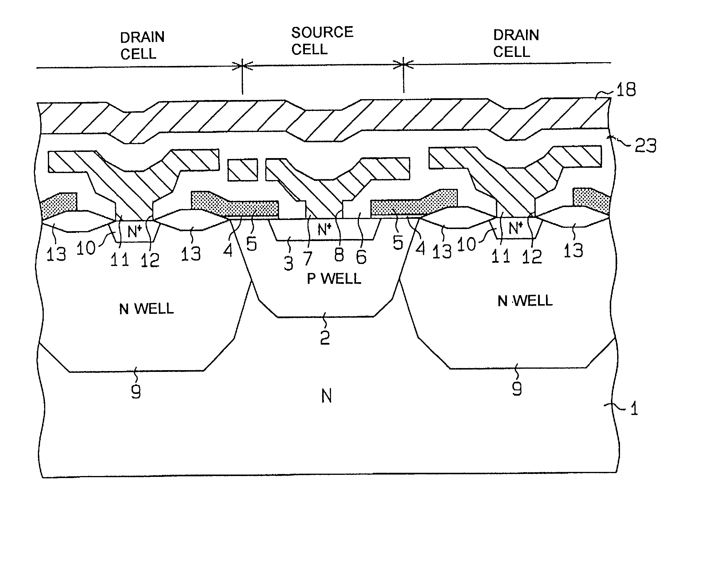
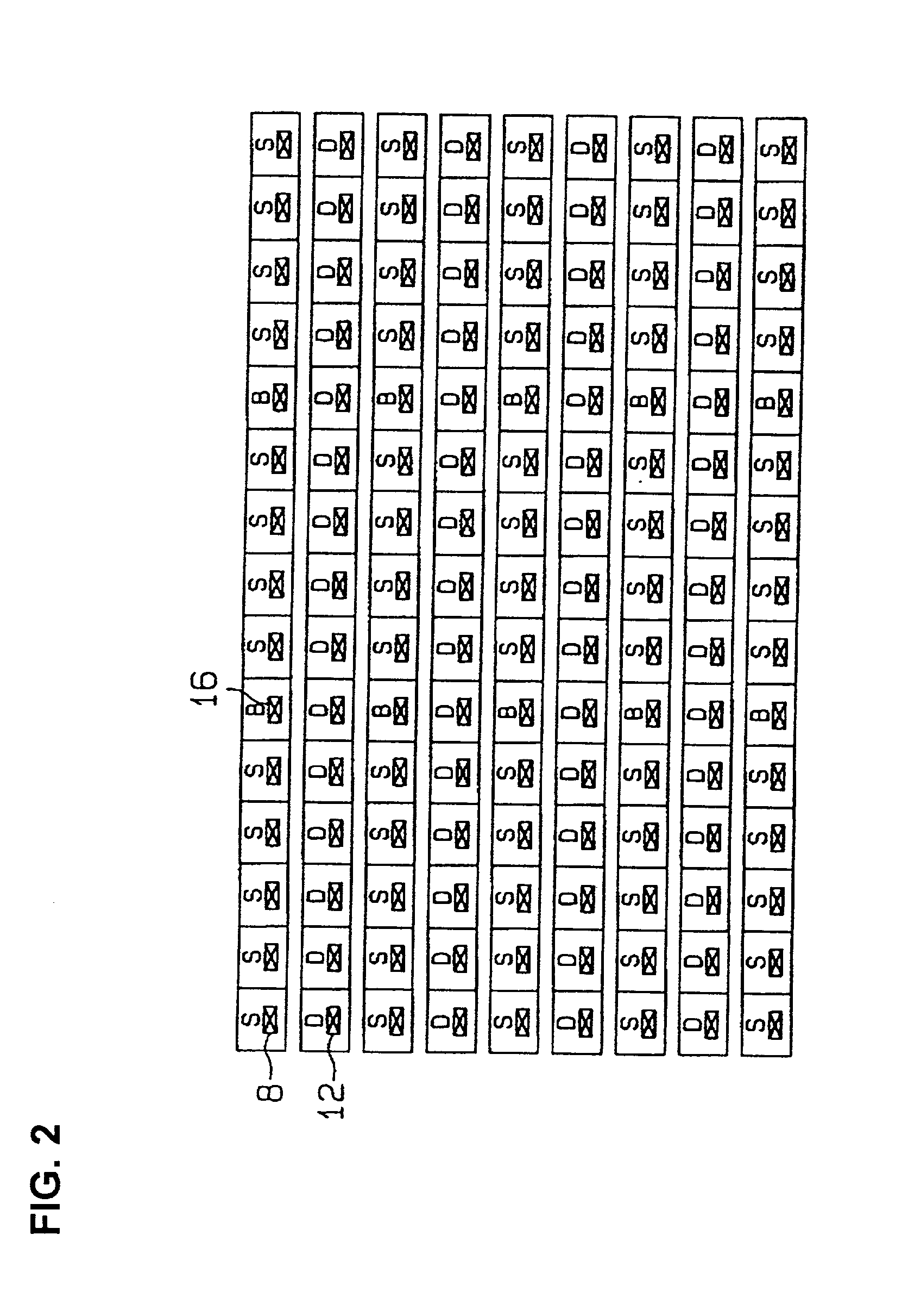
[0067] FIG. 9 shows an embodiment which constitutes an IC chip 45 on which a power MOS (LDMOS) transistor having the configuration of the first embodiment described above, designated as Tr1, is formed in conjunction with a gate drive circuit 30 and a substrate bias circuit 40. The drain side (specifically, the second-layer drain connecting lead 19 of the power MOS transistor Tr1 is connected to a load 44 which is external to the chip 45, while the source side of the power MOS transistor Tr1 (i.e., the second-layer source connecting lead 18) is connected to ground potential. That is to say, the load 44 is connected through the power MOS transistor Tr1 between the high potential of a power source and ground potential of that power source. The gate drive circuit 30 includes a buffer amplifier 31 and a transistor drive command signal (i.e., transistor ON / OFF switching signal) .phi..sub.0 inputted to the gate electrode of the power MOS transistor Tr1 through the buffer amplifier 31. The ...

third embodiment

[0073] A third embodiment is illustrated in the circuit diagram of FIG. 10, in which a power MOS transistor Tr1 configured in accordance with the present invention and a substrate bias circuit 50 are formed on an IC chip 46, with the power MOS transistor Tr1 driving an external load 44. This embodiment differs from that of FIG. 9 in that the substrate bias circuit 50 utilizes the fact that, when a reverse bias is applied to the substrate, the threshold voltage Vt of the power MOS transistor Tr1 is increased due to the substrate effect. Hence, the substrate bias circuit 50 can be used to control the value of Vt. Specifically, when the power MOS transistor Tr1 is in the OFF state (i.e., with 0 V applied as the gate voltage), a reverse bias is applied to the substrate (e.g., having a value of several pad volts, which is of positive polarity in the case of the N-MOS structure) causing the threshold voltage Vt of transistor Tr1 to become high. When transistor Tr1 is set in the ON state (...


PUM


Abstract

A power MOS transistor formed of an array of source cells and drain cells on an IC chip substrate has a plurality of substrate contact cells, each formed external to the source cells, having respective substrate potential-setting electrodes to which an externally supplied substrate bias voltage can be applied, enabling the substrate potential to be set independently of the source potential of the transistor. It thereby becomes possible to modify the threshold voltage of the transistor or maintain a constant potential difference between the substrate potential and that of a gate input signal. Since the requirement for a substrate contact region within each source cell is eliminated, and the number of substrate contact cells can be fewer than that of the source cells, the chip area occupied by the transistor can be reduced by comparison with a prior art configuration providing such a substrate potential control capability.

Description

[0001] 1. Field of the Invention[0002] The present invention relates to a power MOS transistor capable of passing a high level of drain current, which is formed of an array of MOSFET (metal-oxide-semiconductor field effect transistor) cells.[0003] 2. Description of the Prior Art[0004] Types of LDMOS FET (lateral diffusion MOSFET, referred to in the following as a LDMOS transistor), formed of an array of interconnected MOSFET cells to constitute a power MOS transistor, are known in the prior art. Such a transistor has a multi-layer configuration of connecting leads, to thereby enable the area occupied by the connecting leads to be reduced and to enable the wiring resistance within the transistor to be lowered. An example of such a prior art LDMOS transistor configuration is shown in FIGS. 20 and 21. As illustrated in the plan view of FIG. 20, this has a conventional stripe configuration of MOSFET cells (source cells and drain cells). The respective source electrodes of the source cel...

Claims


Application Information

Patent Timeline
Patent Type & Authority Applications(United States)
IPC IPC(8): H01L29/08H01L29/10H01L29/78
CPCH01L29/0696H01L29/0847H01L29/1087Y10S257/901H01L29/7802H01L29/7816H01L29/7835H01L29/1095H01L29/7811H01L23/4824
Inventor NAKANO, TAKASHISHIRAKI, SATOSHIFUKUDA, YUTAKAUEDA, NOBUMASAMIURA, SHOJI
Owner DENSO CORP
Why Eureka
Try Eureka