Polishing pad for use in chemical - mechanical palanarization of semiconductor wafers and method of making same

Inactive Publication Date: 2002-09-12
RAYBESTOS POWERTRAIN +2
View PDF20 Cites 26 Cited by
  • Summary
  • Abstract
  • Description
  • Claims
  • Application Information

AI Technical Summary

Benefits of technology

[0010] It is, therefore, the primary objective of the present invention to provide a novel polishing pad for chemical mechanical planarization of semiconductor wafers and similar materials that eliminates the need for pad conditioning.
[0012] The polishing pad for chemical mechanical planarization of semiconductor wafers and similar materials of the invention eliminates the need for the pad conditioning required of prior-art polishing pads. The polishing pad of the present invention does not undergo plastic deformation during use, and retains its original polishing characteristics, thus extending life of the polishing pad.
[0015] Another feature of polishing pad of the invention is its polishing surface. In prior art processes, where diamond grit conditioning pads traverse the surface of a polishing pad, material is actually removed from the polishing pad surface. Random surface asperities are created on the polishing pad's surface. The creation of surface asperities at the same time creates random flow channels around these surface asperities that significantly improves polishing slurry distribution. Pad conditioning is a type of surface grinding. In the polishing pad of the present invention, the polishing pad's surface or surfaces are ground when the pad is first produced. Because of the polishing pad of the invention uses a thermoset phenolic resin, this structure containing asperities is retained even after continuous polishing. Surface asperities of at least 10 microns in height, width or length have shown excellent performance results.
[0017] The porous nature of the polishing pad of the present invention also provides spaces or interstices in which used slurry and polishing debris are stored, which are subsequently rinsed away when necessary or desired, in order to further enhance the effectiveness of the polishing operation.

Problems solved by technology

Features that protrude into another layer and make contact where not intended or do not make contact where intended can cause short circuits, open circuits and other defects that make a valuable product unusable.
Otherwise, small surface irregularities can cause defects, and an extremely valuable part can be defective and lost.
One problem with this approach has been changes in the rate of removal over the life of the polishing pad.
The polishing surface of these pads tends to become glazed and worn over time during the polishing operation on multiple wafers.
This changes the pad's surface characteristics sufficiently to cause the polishing performance to deteriorate significantly over time.
Unfortunately, pad conditioning actually removes material from the polishing pad surface so that over time the polishing pad is slowly ground away, thus shortening the polishing pad's life.
While this has solved the problem of glazing and subsequent variation in rate of removal, it has introduced a new problem: To wit, the shortening of pad life.
Pad conditioning has significantly reduced pad life with the resulting increase in cost of ownership.
In addition, abrasive particles from the slurry and polishing debris embed themselves into the soft surface of the thermoplastic polishing pad, creating a glazed surface that no longer retains its original polishing characteristics.
Another problem inherent with pad conditioning systems is the cost of maintenance, and the cost of the diamond grit conditioning pads.
In addition, diamond particles sometimes come loose from the conditioning pad and cause scratches on the wafer that cannot be repaired, adding substantially to the cost of ownership.

Method used


Image

  • Polishing pad for use in chemical - mechanical palanarization of semiconductor wafers and method of making same
  • Polishing pad for use in chemical - mechanical palanarization of semiconductor wafers and method of making same
  • Polishing pad for use in chemical - mechanical palanarization of semiconductor wafers and method of making same

Examples


Embodiment Construction

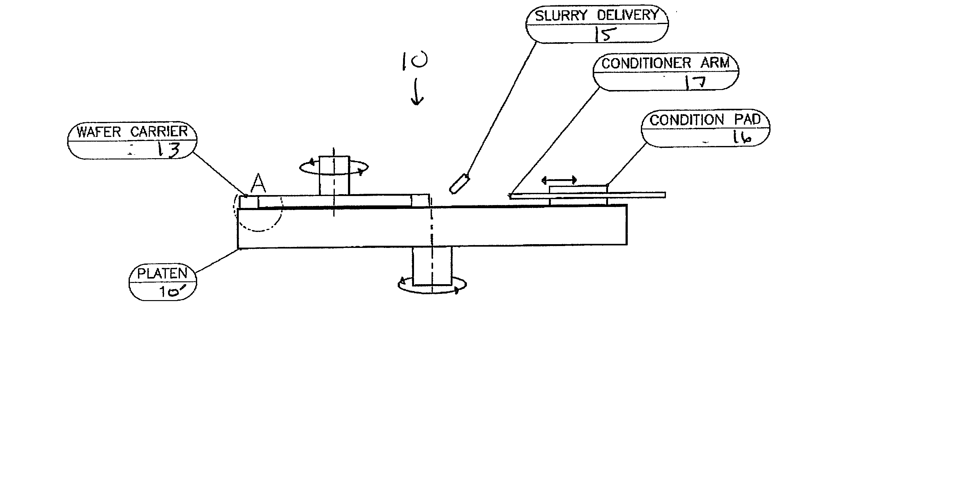
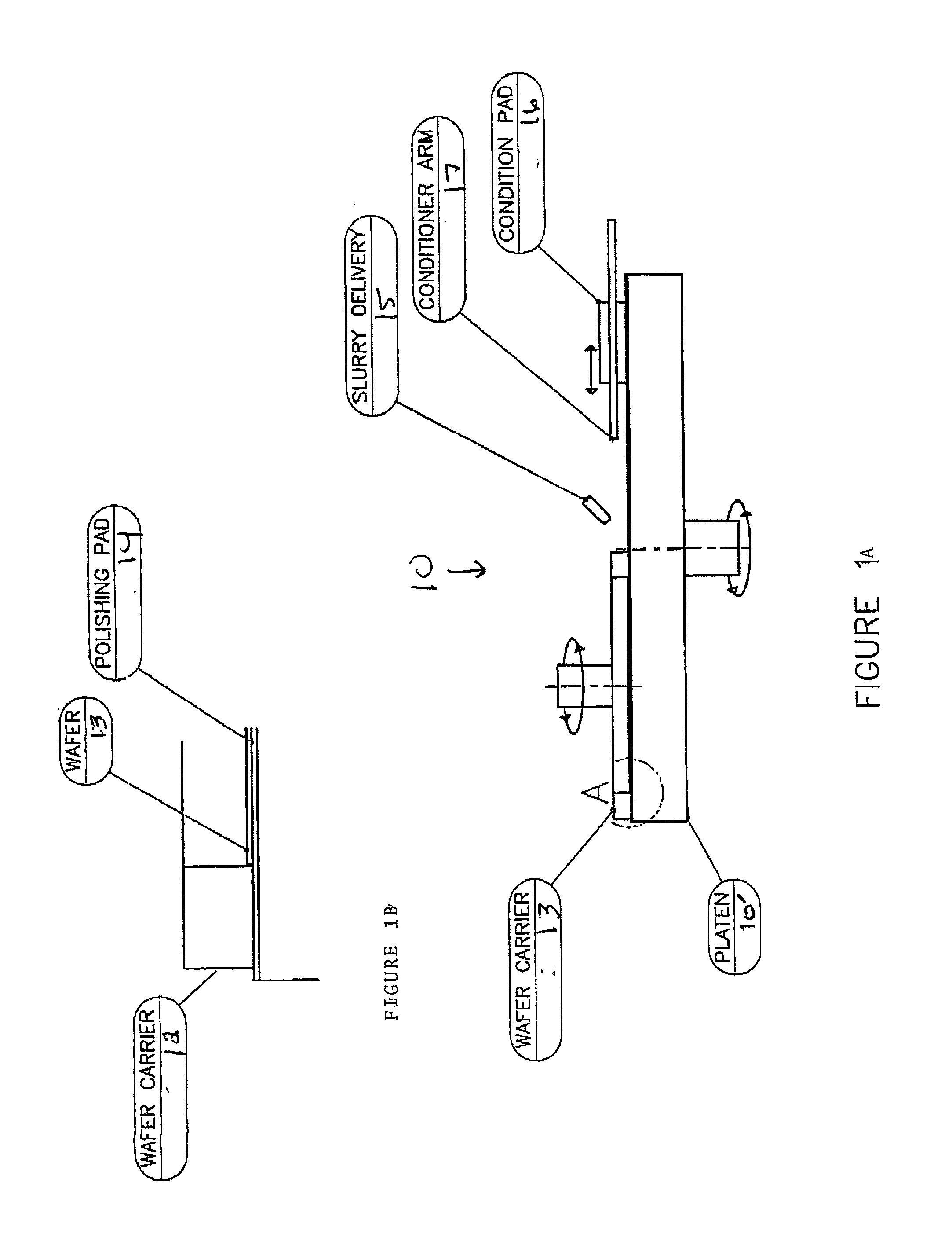
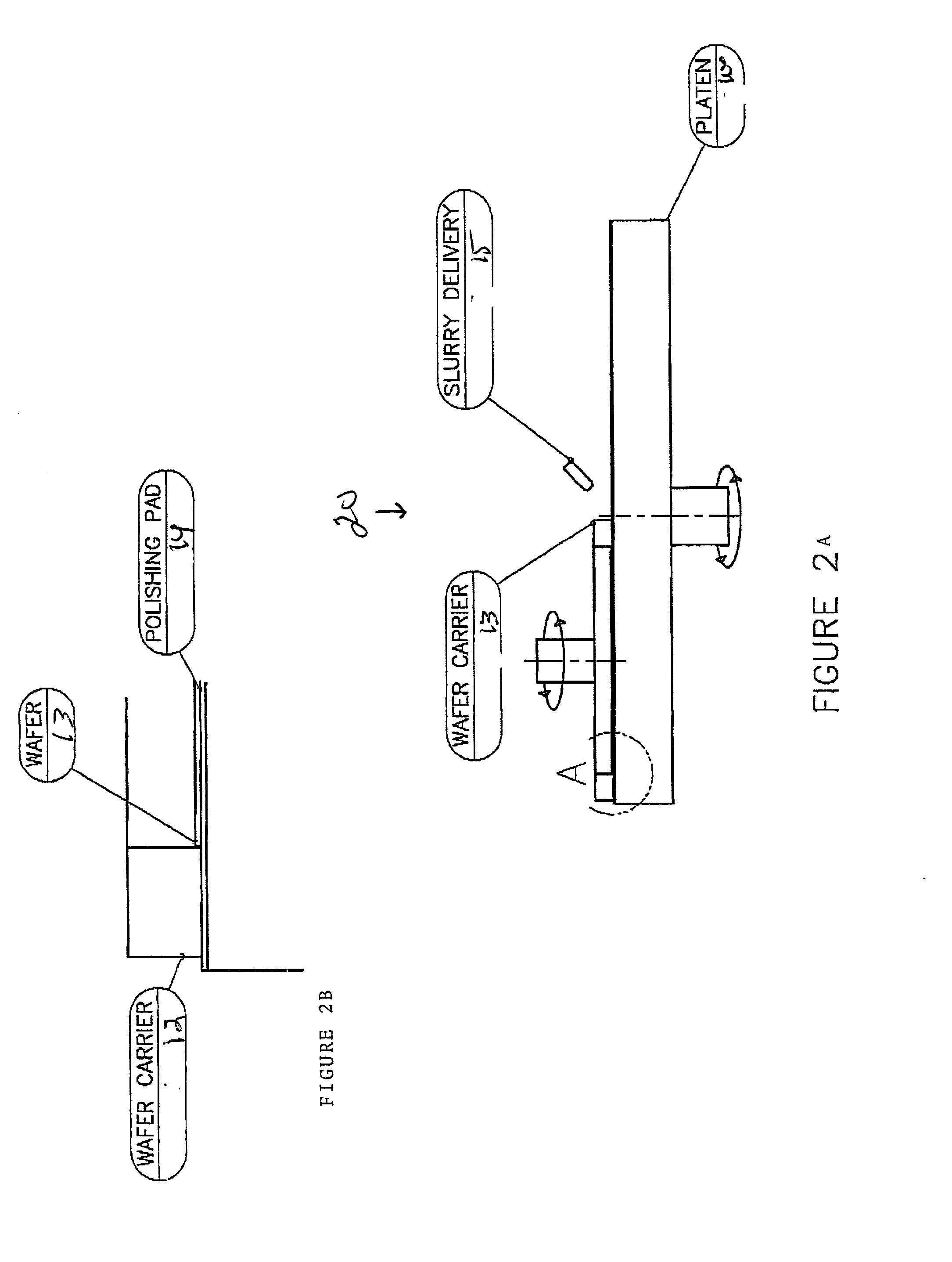
[0025] The polishing pad for polishing or planarizing semiconductor wafers and similar materials of the present invention is a three dimensional, porous fiber structure that is impregnated and bound together with a thermoset resin that is creep-resistant, and ground on one or both surfaces thereof in order to produce asperities therein. The polishing pad's asperities may be in the range of between 5 and 50 microns, with a preferred range of between 10 and 25 microns. These asperities provide random flow channels for the flow therein of polishing slurry. The surface may also be grooved in order to enhance the flow of the polishing slurry.

[0026] The polishing pad is a matrix of absorbent fibers impregnated with a thermoset resin, preferably phenolic, is densified, grooved, if required, and cured to provide a rigid, yet porous structure. Other thermoset resins may be used, such as silicones, epoxies, blends thereof, and the like. The fibers that may be used are: natural or synthetic in...


PUM

PropertyMeasurementUnit
Lengthaaaaaaaaaa
Lengthaaaaaaaaaa
Lengthaaaaaaaaaa

Abstract

A polishing pad for use in chemical mechanical polishing of substrates that being made of fibrous matrix such as cellulose with a binder consisting of thermoset resin material, such as phenolic resin. The polishing surface is ground to form asperities. The polishing pad provides a porous structure by which polishing slurry and polishing debris during chemical mechanical polishing of substrates are stored for subsequent rinsing away, and for enhanced flow-distribution of the polishing slurry. Also disclosed is a method of making the polishing pad.

Description

CROSS REFERENCE TO RELATED APPLICATION[0001] Priority of provision application serial No. 60 / 274,121, filed on Mar. 8, 2001, is herewith claimed.BACKGROUND OF THE INVENTION[0002] The present invention is directed to a polishing pad for the chemical-mechanical planarization of semiconductor wafers and a method of making it. Semiconductor wafers may have multiple layers of wiring devices on a single wafer. These wiring devices consist of hundreds of electrical circuits fabricated and interconnected in order to produce the computer chips that will eventually be die cut from the wafer. These wiring devices are called integrated circuits (IC). A layer of insulating materials, often silicon dioxide (S.sub.1O.sub.2), separate each layer of integrated circuits so that designated IC's interconnect. In order to pack more devices into less space, the requirements for feature size within the IC's has shrunk dramatically. There may now be feature sizes smaller than 0.01 microns. As layers of int...

Claims


Application Information

Patent Timeline
IPC IPC(8): B24B37/24B24D3/32B24D13/14
CPCB24B37/24B24D3/32
Inventor COOPER, RICHARD D.FATHAUER, PAULMROCZEK-PETROSKI, ANGELA MROCZEKPERRY, DAVID
Owner RAYBESTOS POWERTRAIN
Why Eureka
Try Eureka