Layout design system and layout design method
a layout design and layout technology, applied in the field of layout design systems and layout design methods, can solve the problems of long operating time and achieve the effect of short period of time and short period of tim
- Summary
- Abstract
- Description
- Claims
- Application Information
AI Technical Summary
Benefits of technology
Problems solved by technology
Method used
Image
Examples
embodiment 1
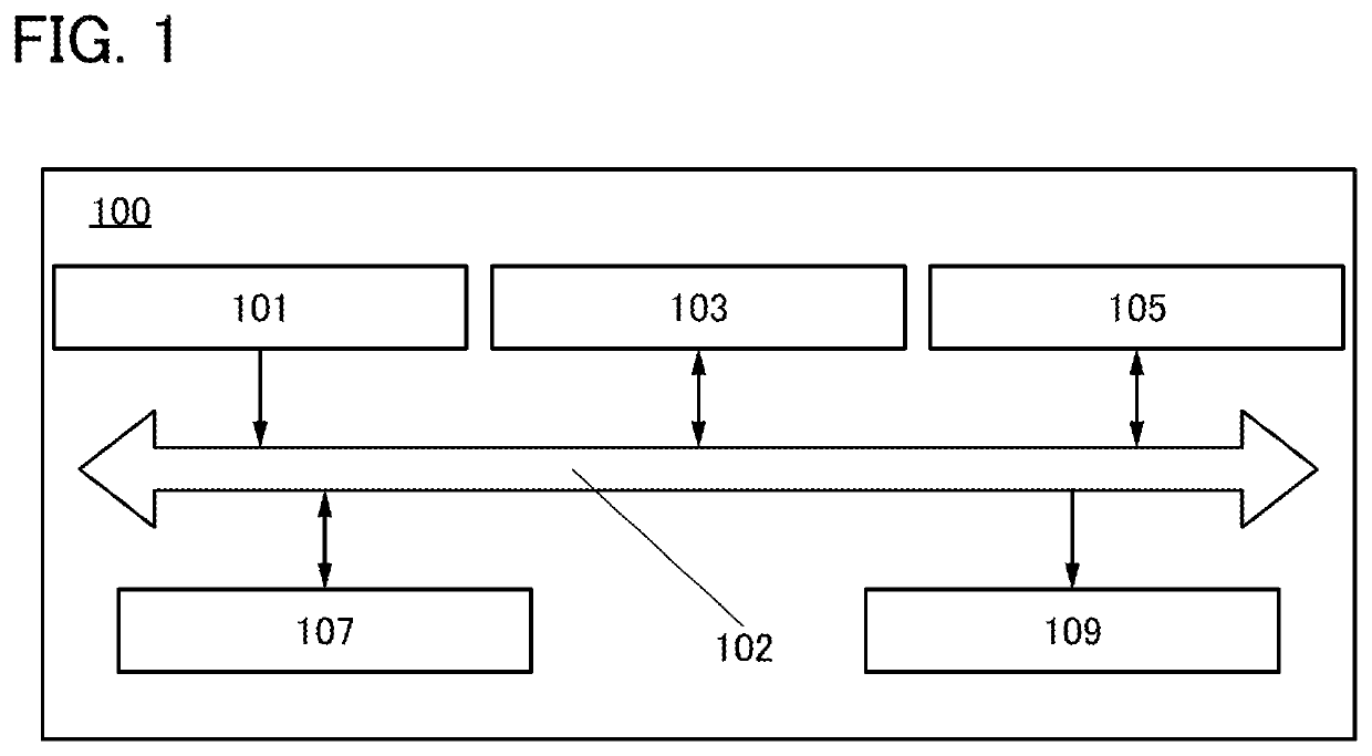
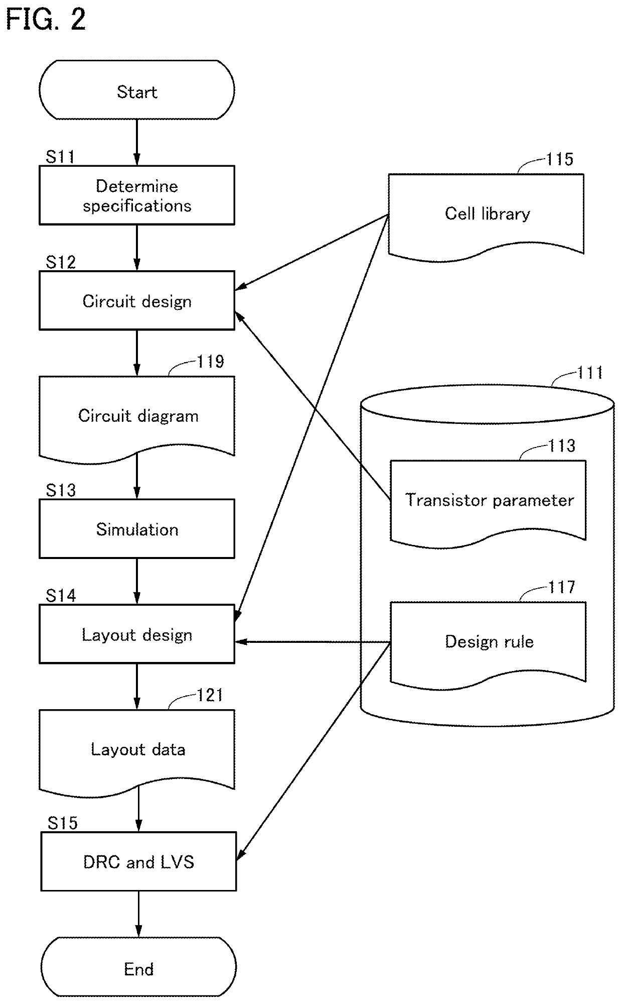
[0058]In this embodiment, a layout design system of one embodiment of the present invention is described with reference to FIG. 1 to FIG. 26.
[0059]A layout design system that is one embodiment of the present invention has a function of generating layout data on the basis of a circuit diagram and layout design information. The layout design system that is one embodiment of the present invention can be used for layout design of an integrated circuit.
[0060]In this specification and the like, layout design means generating layout data on the basis of a circuit diagram and layout design information. The circuit diagram is a diagram which expresses connection of active elements such as a transistor and a diode and passive elements such as a capacitor and a resistor with the use of figures and lines. The layout data is information on the shape and arrangement of a semiconductor layer, a conductor layer, or the like which is transferred to a mask (also referred to as a reticle). Note that i...
embodiment 2
[0242]In this embodiment, structure examples of a semiconductor device that can be used in the neural networks described in the above embodiment are described.
[0243]As illustrated in FIG. 27(A), a neural network NN can be formed of an input layer IL, an output layer OL, and a middle layer (hidden layer) HL. The input layer IL, the output layer OL, and the middle layer HL each include one or more neurons (units). Note that the middle layer HL may be composed of one layer or two or more layers. A neural network including two or more middle layers HL can also be referred to as a DNN (deep neural network), and learning using a deep neural network can also be referred to as deep learning.
[0244]Input data is input to neurons of the input layer IL, output signals of neurons in the previous layer or the subsequent layer are input to neurons of the middle layer HL, and output signals of neurons in the previous layer are input to neurons of the output layer OL. Note that each neuron may be co...
example
[0316]In this example, layout design was performed using the method described in .
[0317]In this example, a grid had a grid interval of 1 and a grid frame size of 20×20 (grid area: 400). Four abstracts were used and each abstract had a size of 3×3.
[0318]In Step S27 and Step S32, the discount rate γ was 0.95 in updating of the action value function Q(st,at). The first neural network and the second neural network were optimized using Adam. The movement a was selected using an ε-greedy method. In one episode, ε was 1; after that, c was linearly decreased so that c was 0.1 in 80000 episodes. After 80000 episodes, c was 0.1.
[0319]In Step S33, the reward for a movement of an abstract was 1−(block area / 400), and setting was such that the reward decreased as the block area increased. In Step S36, the reward was 0 in the case where the connection points were able to be connected and the design rule was satisfied, and the reward was −1 in the case where the connection points were not able to b...
PUM
 Abstract
Description
Claims
Application Information
 - R&D
- Intellectual Property
- Life Sciences
- Materials
- Tech Scout
- Unparalleled Data Quality
- Higher Quality Content
- 60% Fewer Hallucinations
Browse by: Latest US Patents, China's latest patents, Technical Efficacy Thesaurus, Application Domain, Technology Topic, Popular Technical Reports.
© 2025 PatSnap. All rights reserved.Legal|Privacy policy|Modern Slavery Act Transparency Statement|Sitemap|About US| Contact US: help@patsnap.com


