Semiconductor contact structure having stress buffer layer formed between under bump metal layer and copper pillar

a contact structure and buffer layer technology, applied in the direction of semiconductor devices, semiconductor/solid-state device details, electrical devices, etc., can solve the problems of product failure, dielectric layer and wiring easily delaminated, and current conventional under bump metal layer is not enough to significantly reduce thermo-mechanical stress, etc., to achieve the effect of improving thermal-mechanical stress, high thermal expansion of copper, and improving the cracking caused by the difference in thermal expansion coefficient between materials

Active Publication Date: 2021-01-26
UNITED MICROELECTRONICS CORP
View PDF10 Cites 3 Cited by
  • Summary
  • Abstract
  • Description
  • Claims
  • Application Information

AI Technical Summary

Benefits of technology

[0004]The present invention provides a semiconductor apparatus and a method for manufacturing the same, which solve the problem of delamination defects and cracks which are easily generated in the semiconductor apparatus.
[0022]In the present invention, by arranging the stress buffer layer between the copper pillar and the under bump metal layer, the higher thermal-mechanical stress on the semiconductor apparatus, which is caused by higher Young's modules and high thermal expansion of the copper, can be effectively reduced to prevent from the IMD (inter-metal dielectric) delamination, and the problem of cracks caused by the difference in thermal expansion coefficient between materials can also be improved.

Problems solved by technology

The copper pillar is usually disposed on the under bump metal layer, but the current conventional under bump metal layer is not enough to significantly reduce the thermo-mechanical stress.
Therefore, in the semiconductor package component having the copper pillar, the adhesion between the copper-plated wiring and the polymer dielectric layer is not good, so as to cause the defect that the polymer dielectric layer and the wiring are easily delaminated.
Not only the delamination defect causes the product to fail in the long-term reliability test, but also the crack between the wire and the polymer dielectric layer is occur in the reliability thermal cycling test (TCT) process because of the difference in thermal expansion coefficient between materials, so as to affect the function and lifetime of the product.

Method used


Image

  • Semiconductor contact structure having stress buffer layer formed between under bump metal layer and copper pillar
  • Semiconductor contact structure having stress buffer layer formed between under bump metal layer and copper pillar
  • Semiconductor contact structure having stress buffer layer formed between under bump metal layer and copper pillar

Examples


Embodiment Construction

[0033]The present invention will now be described more specifically with reference to the following embodiments. It is to be noted that the following descriptions of preferred embodiments of this invention are presented herein for purpose of illustration and description only. It is not intended to be exhaustive or to be limited to the precise form disclosed.

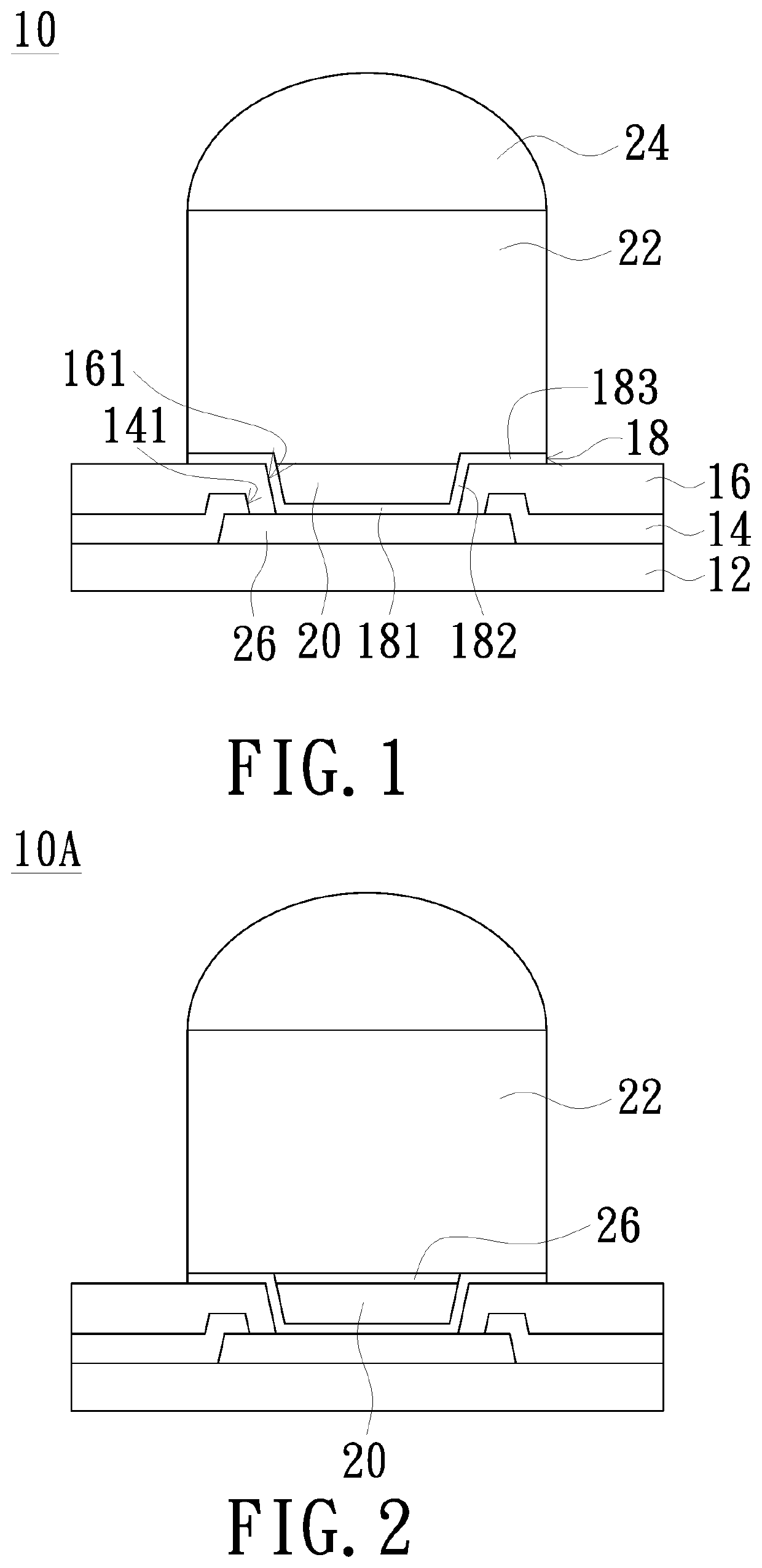
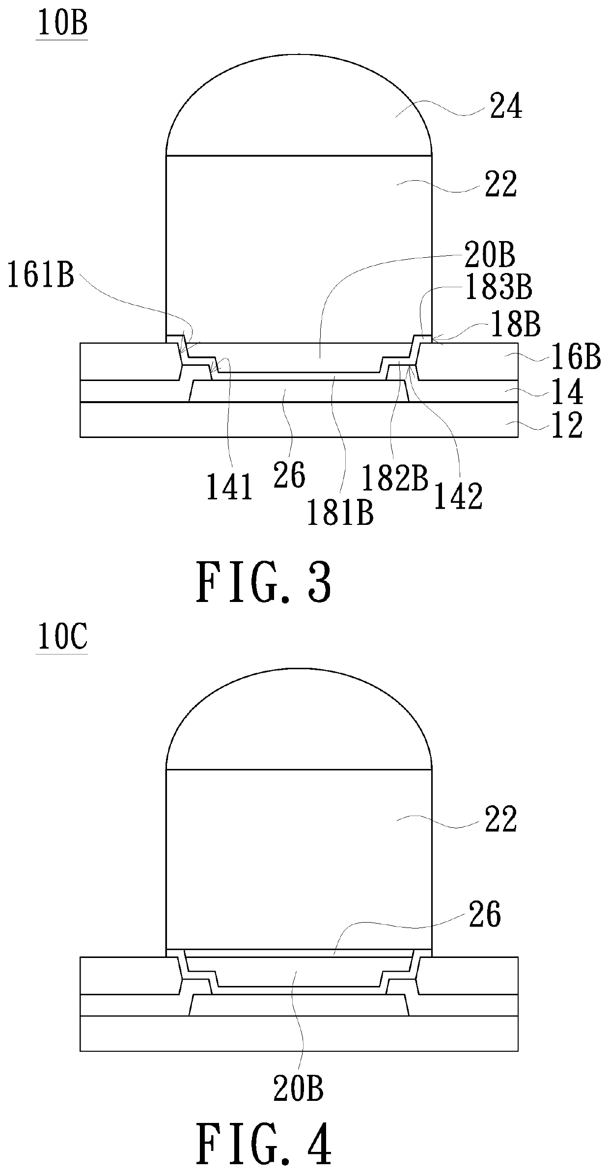
[0034]FIG. 1 is a schematic structural diagram of a semiconductor apparatus according to a first embodiment of the present invention. As shown in FIG. 1, the semiconductor apparatus 10 includes a semiconductor substrate 12, a first passivation layer (PASV) 14, a second passivation layer (re-passivation layer, Re-PASV) 16, an under bump metal (UBM) layer 18, a stress buffer layer 20, a copper pillar 22 and a solder structure 24.

[0035]The semiconductor substrate 12 has at least one metal pad 26 thereon. The semiconductor substrate 12 may be a silicon wafer or a layer of silicon-containing material, and integrated circuits may be fo...


PUM

PropertyMeasurementUnit
heightaaaaaaaaaa
heightaaaaaaaaaa
heightaaaaaaaaaa

Abstract

Semiconductor apparatus and method for manufacturing semiconductor apparatus are provided. Semiconductor apparatus includes a semiconductor substrate having metal pads, a first passivation layer, a second passivation layer, an under bump metal layer, a stress buffer layer, a copper pillar and a solder structure. First passivation layer is formed on the semiconductor substrate and covers a portion of each metal pad, the first passivation layer has first passivation layer openings to expose a first portion of each metal pad. Second passivation layer is formed on the first passivation layer, the second passivation layer has second passivation layer openings to expose a second portion of each metal pad. Under bump metal layer is formed on the second portion of each metal pad exposed by the second passivation layer opening. Stress buffer layer is formed on the under bump metal layer, and the copper pillar is disposed on the stress buffer layer.

Description

FIELD OF THE INVENTION[0001]The present invention relates to a semiconductor technology, and more particularly to a semiconductor apparatus having copper pillar structures and a method for manufacturing the semiconductor apparatus.BACKGROUND OF THE INVENTION[0002]The integrated circuit is made up of millions of active devices which are initially isolated from each other and then connected by interconnects to form functional circuits. In the flip-chip packaging technology, in order to obtain fine pitches, copper-pillar bump structures are often used as connection structures for connecting the interconnect structures to the package surface or other dies, wherein a metal pad is disposed on the contact of each interconnect structure. The conventional copper-pillar bump structure mainly includes an under bump metal (UBM) layer, a copper pillar and a solder cap on the copper pillar.[0003]Generally, copper has good electrical conductivity, thermal conductivity and excellent electromigratio...

Claims


Application Information

Patent Timeline
Patent Type & Authority Patents(United States)
IPC IPC(8): H01L23/00
CPCH01L24/05H01L24/03H01L24/11H01L24/13H01L2224/02181H01L2224/03462H01L2224/03912H01L2224/0401H01L2224/05018H01L2224/05019H01L2224/05083H01L2224/05084H01L2224/05109H01L2224/05111H01L2224/05139H01L2224/05147H01L2224/05155H01L2224/05166H01L2224/05181H01L2224/05184H01L2224/11462H01L2224/11825H01L2224/13006H01L2224/1357H01L2224/13147H01L2924/35121H01L24/10H01L2224/10122H01L2224/10125H01L2224/13014H01L2224/13019H01L2224/13021H01L2224/13082H01L2224/05564H01L2224/05541H01L2224/131H01L2224/05559H01L2224/16227H01L2224/16237H01L24/20H01L2224/12105H01L2224/04105H01L2224/18H01L2224/1147H01L2224/0347H01L2224/11903H01L2224/0345H01L2224/05611H01L2224/05609H01L2224/11849H01L2224/119H01L2224/0361H01L24/16H01L23/562H01L23/3192H01L2224/05578H01L2224/05576H01L2224/05547H01L2224/05639H01L2224/13139H01L2224/05666H01L2224/05681H01L2224/13111H01L2224/81399H01L2224/05124H01L2224/05655H01L2924/381H01L2924/3512H01L2924/00014H01L2924/00012H01L2924/014H01L2924/0001H01L2924/01047H01L2224/034H01L2924/013H01L2924/0105H01L2924/01074H01L2924/01022
Inventor LIN, YU-JIE
Owner UNITED MICROELECTRONICS CORP
Why Eureka
Try Eureka