Miniature ultrasonic imaging system
a technology of ultrasonic imaging and micro-machine, applied in ultrasonic/sonic/infrasonic image/data processing, mechanical vibration separation, application, etc., can solve the problems of multiple error sources, lack of fitness usage devices capable of monitoring local muscle building effectiveness, and currently available blood pressure gauge devices (sphygmomanometers) are difficult to use without calibration and proficiency training, and achieve the effect of facilitating cosmetic supervision
- Summary
- Abstract
- Description
- Claims
- Application Information
AI Technical Summary
Benefits of technology
Problems solved by technology
Method used
Image
Examples
embodiment 10
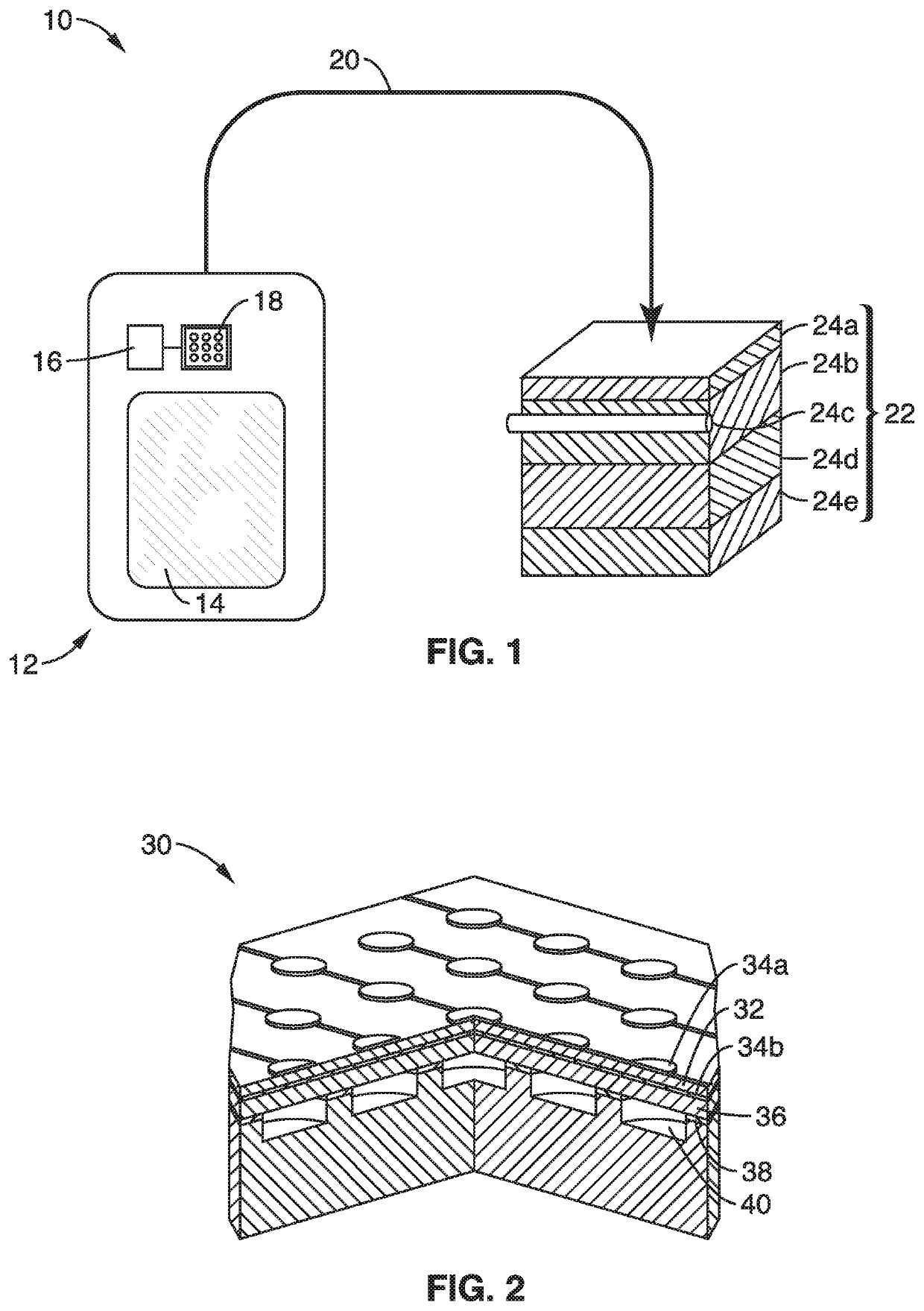
[0031]FIG. 1 illustrates an embodiment 10 of an ultrasonic imaging system. By way of example, a portable device 12, having display 14 (e.g., touch screen) is shown with an ultrasonic imager circuit to emit ultrasonic waves. Display screen 14 may also provide touch input for user I / O, such as for supporting a graphical user interface (GUI), or other user interfacing. The ultrasonic imager comprises an ultrasonic imaging sensor array 18 coupled to a processor 16, such as within an application specific integrated circuit (ASIC), which may be coupled to (mounted upon) the portable electronic device and / or integrated within it.
[0032]During operation, the user contacts the imager 18, to a local body part area 22, upon which ultrasonic wave are emitted (transmitted) into that area of the patient's body. Arrow 20 merely represents the movement of imager 18 to achieve contact with body area 22. The imager collects (receives) the reflected sound wave signal and the processor processes the ima...
embodiment 30
[0036]In FIG. 2 a cutaway of a PMUT embodiment 30 is shown having a piezoelectric layer 32, over which is disposed a top electrode pattern 34a. Beneath the piezoelectric layer 32 there is shown a bottom electrode 34b, and a device semiconductor 36 (e.g., Si depicted by way of example), followed by dielectric regions 38 (e.g., SiO2), and cavities 40.
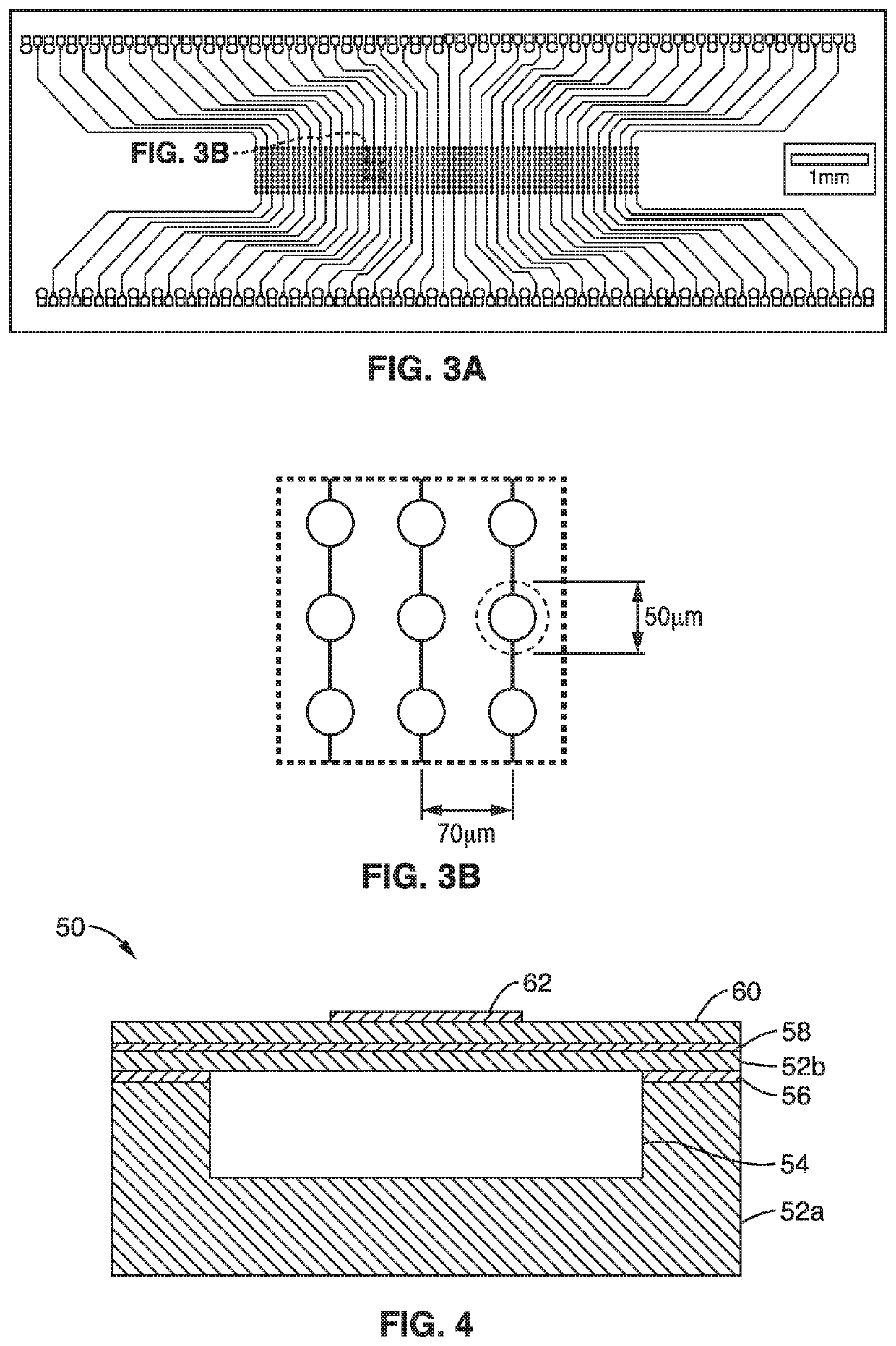
[0037]FIG. 3A and FIG. 3B show a trace pattern of a PMUT ASIC as seen in FIG. 3A, with electrode areas magnified in FIG. 3B, shown with example electrode area of 50 μm, and a pitch (spacing between electrodes) of 70 μm.
embodiment 50
[0038]FIG. 4 illustrates an embodiment 50 of a PMUT showing a single electrode 62 over a cavity region 54. A material substrate 52a (e.g., Si) is shown into which a cavity 54 is formed, typically by a subtractive process (i.e., etching), over which is deposited a dielectric layer 56 (e.g., SiO2), above which is another material layer 52b (e.g., Si), bottom electrode 58, piezoelectric layer 60, upon which electrode 62 is disposed.
[0039]FIG. 5 illustrates an an ultrasonic sensor 70 comprising a low voltage supply 72 and digital control block 74 supplying power and control to an ASIC array 76, shown coupled to a PMUT transducer array 77. Output from ASIC 76 is shown being received at an analog-to-digital converter (ADC) 78 before receipt by at least one processing element 80 which processes the ultrasonic data to generate image data, which can be processed as an image output 82 directed to a display. It should also be recognized that the image data can be processed to extract salient f...
PUM
 Abstract
Description
Claims
Application Information
 - R&D
- Intellectual Property
- Life Sciences
- Materials
- Tech Scout
- Unparalleled Data Quality
- Higher Quality Content
- 60% Fewer Hallucinations
Browse by: Latest US Patents, China's latest patents, Technical Efficacy Thesaurus, Application Domain, Technology Topic, Popular Technical Reports.
© 2025 PatSnap. All rights reserved.Legal|Privacy policy|Modern Slavery Act Transparency Statement|Sitemap|About US| Contact US: help@patsnap.com


