Method of manufacturing embedded magnetoresistive random access memory

a random access memory and random access technology, applied in the direction of magnetic field-controlled resistors, magneticonductor devices, galvano-magnetic material selection, etc., can solve the problem of impaired planarization effect and achieve the effect of better planarization

Active Publication Date: 2020-01-14
UNITED MICROELECTRONICS CORP
View PDF9 Cites 2 Cited by
  • Summary
  • Abstract
  • Description
  • Claims
  • Application Information

AI Technical Summary

Benefits of technology

The invention provides a method of manufacturing an eMRAM with better planarization effect. Specifically, the method includes a process of etch back that removes any remaining second dielectric layer and a portion of the first dielectric layer. Additionally, the method includes two CMP processes, where the metal nitride layer is used as a stop layer during the first CMP process and the second electrode is exposed during the second CMP process. This process provides a smoother surface and better planarization of the eMRAM device.

Problems solved by technology

Therefore, after the dielectric layer is planarized by the chemical mechanical polishing (CMP) method, serious dishing occurs, and the planarization effect is impaired.

Method used


Image

  • Method of manufacturing embedded magnetoresistive random access memory
  • Method of manufacturing embedded magnetoresistive random access memory
  • Method of manufacturing embedded magnetoresistive random access memory

Examples


Embodiment Construction

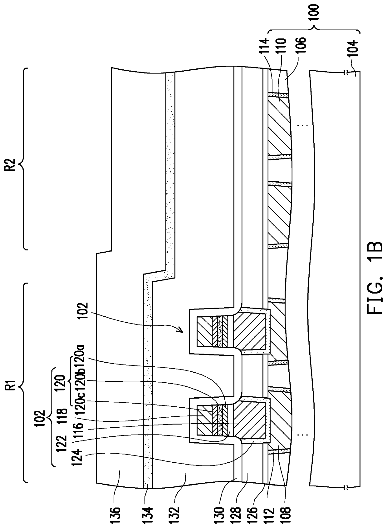
[0030]FIG. 1A to FIG. 1F are cross-sectional views illustrating a manufacturing process of an eMRAM according to an embodiment of the invention.

[0031]Referring to FIG. 1A, a memory cell stack structure 102 is formed on a substrate structure 100. An embedded memory region R1 and a device region R2 adjacent to each other may be defined in the substrate structure 100. The device region R2 is, for example, a logic device region, a RF device region, or a SRAM region. In the present embodiment, the device region R2 is exemplified by the logic device region, but the invention is not limited thereto.

[0032]The substrate structure 100 may include a substrate 104. The substrate 104 may be a semiconductor substrate, such as a silicon substrate. Furthermore, the desired doped region (not shown) and / or the desired semiconductor device (not shown) may be formed in the substrate 104 according to product requirements. In FIG. 1A, the substrate 104 is depicted as a single-layer structure to simplify ...


PUM

PropertyMeasurementUnit
heightaaaaaaaaaa
dielectric constantaaaaaaaaaa
semiconductoraaaaaaaaaa

Abstract

A method of manufacturing an embedded magnetoresistive random access memory including the following steps is provided. A memory cell stack structure is formed on a substrate structure. The memory cell stack structure includes a first electrode, a second electrode, and a magnetic tunnel junction structure. A first dielectric layer covering the memory cell stack structure is formed. A metal nitride layer is formed on the first dielectric layer. A second dielectric layer is formed on the metal nitride layer. A first CMP process is performed on the second dielectric layer to expose the metal nitride layer by using the metal nitride layer as a stop layer. An etch back process is performed to completely remove the metal nitride layer and expose the first dielectric layer. A second CMP process is performed to expose the second electrode. The manufacturing method can have a better planarization effect.

Description

CROSS-REFERENCE TO RELATED APPLICATION[0001]This application claims the priority benefit of China application serial no. 201811050528.4, filed on Sep. 7, 2018. The entirety of the above-mentioned patent application is hereby incorporated by reference herein and made a part of this specification.BACKGROUND OF THE INVENTIONField of the Invention[0002]The invention relates to a method of manufacturing a semiconductor structure, and particularly relates to a method of manufacturing an embedded magnetoresistive random access memory (eMRAM).Description of Related Art[0003]The chip used in the internet of things (IOT) terminal apparatus may include device regions with different functions, such as an embedded memory region, a logic device region, a radio frequency (RF) device region, and a static random access memory (SRAM) region etc.[0004]In the case of using the eMRAM as the embedded memory in the chip, the memory cell stack structure of the eMRAM is formed in the embedded memory region,...

Claims


Application Information

Patent Timeline
Patent Type & Authority Patents(United States)
IPC IPC(8): H01L43/12H01L27/22H01L43/02H01L43/10H01L43/08H10N50/01H10N50/10H10N50/80
CPCH01L43/12H01L27/222H01L43/02H01L43/08H01L43/10H10B61/00H10N50/01H10N50/10H10N50/80H10N50/85
Inventor HUNG, CHING-WENLI, KUN-JU
Owner UNITED MICROELECTRONICS CORP
Why Eureka
Try Eureka