Semiconductor device
a technology of semiconductors and devices, applied in the direction of semiconductor devices, electrical equipment, transistors, etc., can solve the problems of low reliability, achieve high reliability, miniaturize or highly integrated, and avoid the effect of affecting the electrical performan
- Summary
- Abstract
- Description
- Claims
- Application Information
AI Technical Summary
Benefits of technology
Problems solved by technology
Method used
Image
Examples
embodiment 1
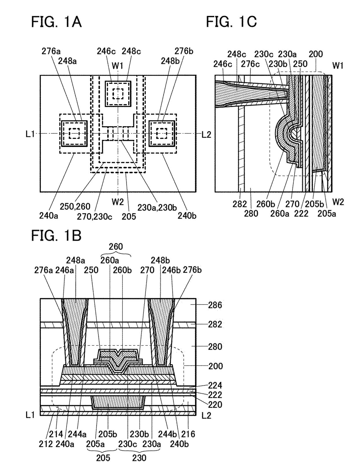
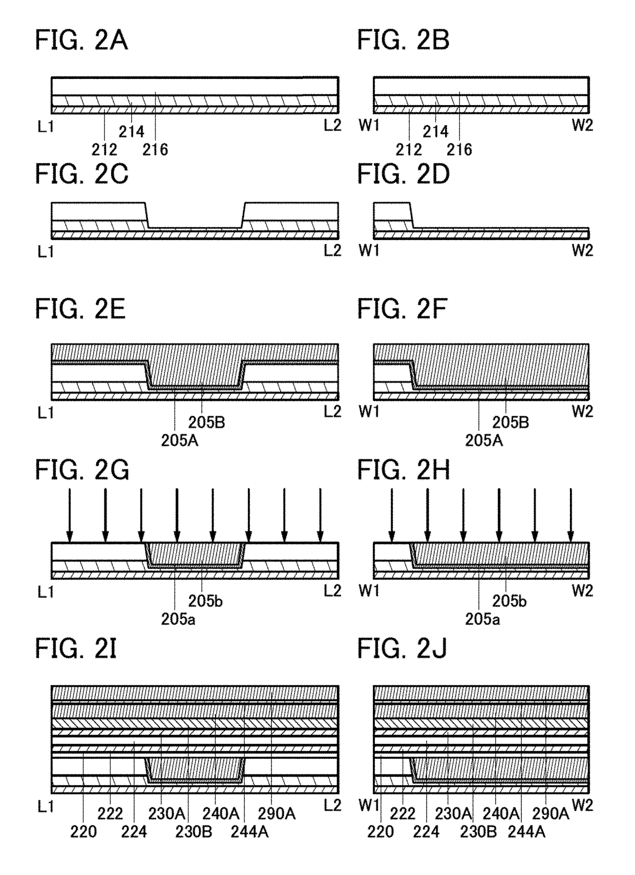
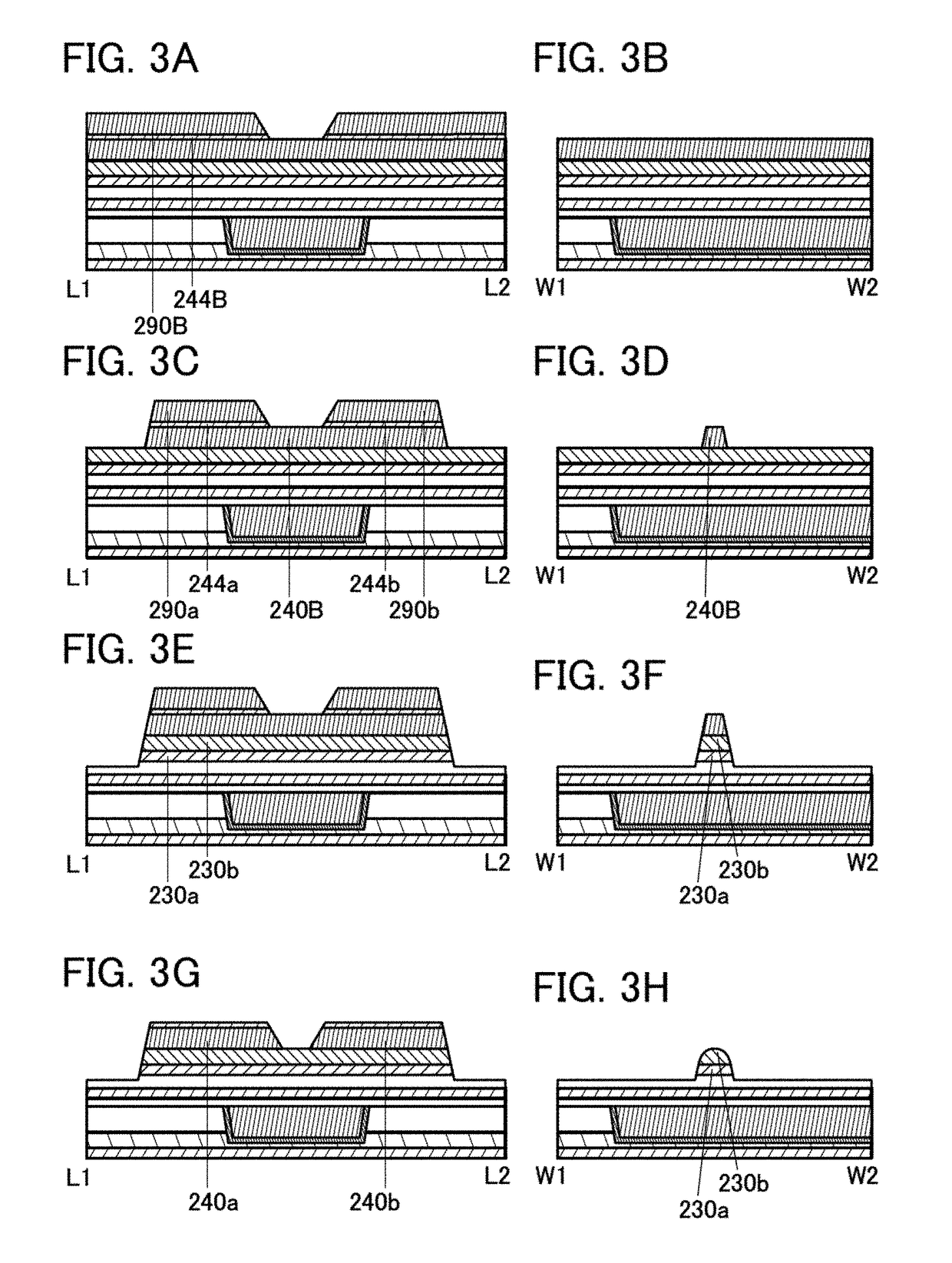
[0077]In this embodiment, one embodiment of a semiconductor device will be described with reference to FIGS. 1A to 1C, FIGS. 2A to 2J, FIGS. 3A to 3H, FIGS. 4A to 4H, FIGS. 5A to 5F, FIGS. 6A to 6D, FIGS. 7A to 7D, FIGS. 8A to 8D, FIGS. 9A and 9B, FIGS. 10A to 10C, and FIGS. 11A to 11C.
[0078]An example of a semiconductor device of one embodiment of the present invention is described below. FIGS. 1A to 1C are a top view and cross-sectional views illustrating a transistor 200 of one embodiment of the present invention and plugs electrically connected to the transistor 200. FIG. 1A is the top view, FIG. 1B is the cross-sectional view taken along a dashed-dotted line L1-L2 in FIG. 1A, and FIG. 1C is the cross-sectional view taken along a dashed-dotted line W1-W2. For simplification of the drawing, some components are not illustrated in the top view in FIG. 1A.
[0079]The semiconductor device of one embodiment of the present invention includes the transistor 200, insulators 280, 282, and 2...
embodiment 2
[0274]In this embodiment, one embodiment of a semiconductor device will be described with reference to FIG. 12, FIG. 13, FIG. 14, and FIG. 15.
[Memory Device 1]
[0275]Examples of a semiconductor device (a memory device) including the transistor 200 that is one embodiment of the present invention are illustrated in FIG. 12, FIG. 13, FIG. 14, and FIG. 15.
[0276]Semiconductor devices illustrated in FIG. 12 and FIG. 13 each include a transistor 300, a transistor 200, and a capacitor 100.
[0277]The transistor 200 is a transistor in which a channel is formed in a semiconductor layer including an oxide semiconductor. Since the off-state current of the transistor 200 is low, by using the transistor 200 in a memory device, stored data can be retained for a long time. In other words, such a memory device does not require refresh operation or has an extremely low frequency of the refresh operation, which leads to a sufficient reduction in power consumption.
[0278]In FIG. 12 and FIG. 13, a wiring 30...
modification example 1
[0335]FIG. 13 illustrates a modification example of this embodiment. FIG. 13 is different from FIG. 12 in the structure of the transistor 300.
[0336]In the transistor 300 illustrated in FIG. 13, the semiconductor region 313 (part of the substrate 311) in which the channel is formed has a protruding portion. Furthermore, the conductor 316 is provided to cover the top and side surfaces of the semiconductor region 313 with the insulator 315 positioned therebetween. Note that the conductor 316 may be formed using a material for adjusting the work function. The transistor 300 having such a structure is also referred to as a FIN transistor because the protruding portion of the semiconductor substrate is utilized. An insulator serving as a mask for forming the protruding portion may be provided in contact with the top surface of the protruding portion. Although the case where the protruding portion is formed by processing part of the semiconductor substrate is described here, a semiconducto...
PUM
 Abstract
Description
Claims
Application Information
 - R&D
- Intellectual Property
- Life Sciences
- Materials
- Tech Scout
- Unparalleled Data Quality
- Higher Quality Content
- 60% Fewer Hallucinations
Browse by: Latest US Patents, China's latest patents, Technical Efficacy Thesaurus, Application Domain, Technology Topic, Popular Technical Reports.
© 2025 PatSnap. All rights reserved.Legal|Privacy policy|Modern Slavery Act Transparency Statement|Sitemap|About US| Contact US: help@patsnap.com


