Chip and packaging structure

A packaging structure and chip technology, applied in the direction of electrical components, electrical solid devices, circuits, etc., can solve the problems of increasing the stress of packaging colloid

Active Publication Date: 2007-06-13
UNITED MICROELECTRONICS CORP
View PDF0 Cites 4 Cited by
  • Summary
  • Abstract
  • Description
  • Claims
  • Application Information

AI Technical Summary

Problems solved by technology

But this move may increase the stress of the encapsulation colloid on the chip, and cause other problems

Method used


Image

  • Chip and packaging structure
  • Chip and packaging structure

Examples


Embodiment Construction

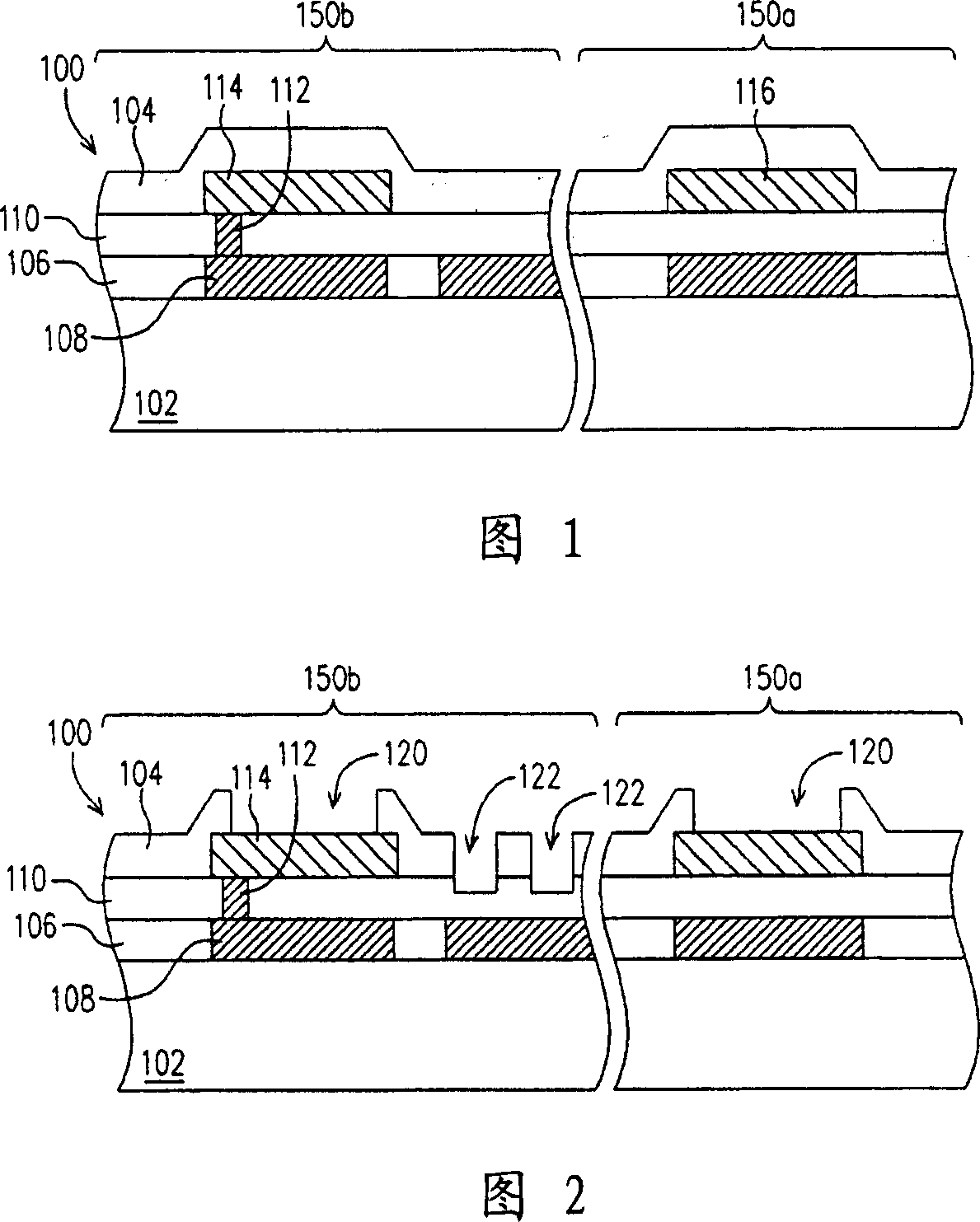
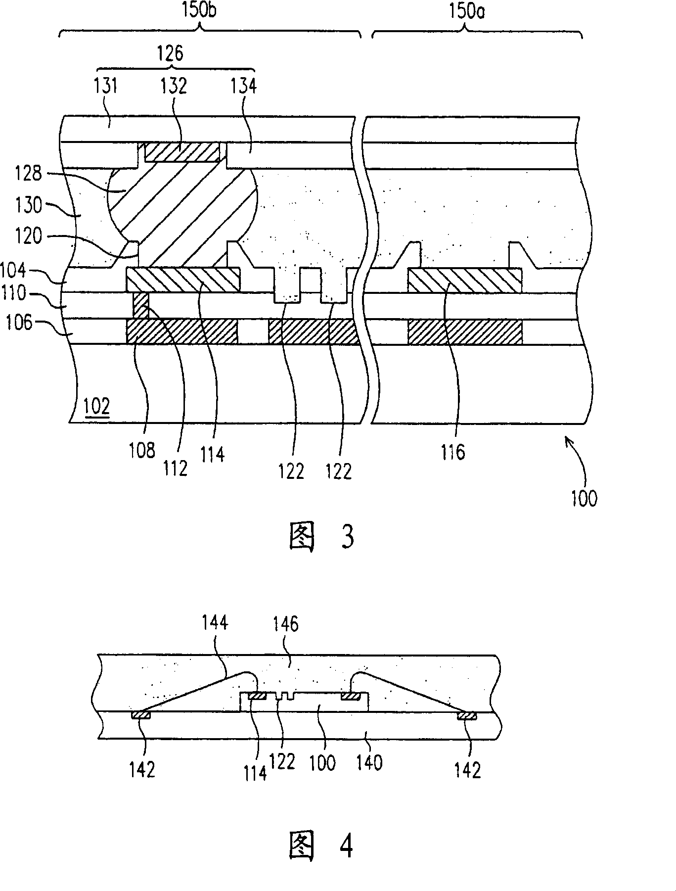
[0041] FIG. 1 to FIG. 2 are cross-sectional views of a manufacturing method of a chip according to an embodiment of the present invention. Referring to FIG. 1 , a chip 100 is provided first. The chip 100 has a substrate 102 and a passivation 104 on the substrate 102 . For the convenience of illustration, FIG. 1 to FIG. 2 only show part of the substrate 102, and the part of the substrate 102 is also configured with a dielectric layer 106, a metal layer 108, a dielectric layer 110, a via (Via) 112, and a solder pad. 114 and fuse pad 116. The material of the dielectric layer 106 is, for example, silicon oxide. The metal layer 108 is disposed in the dielectric layer 106 . The metal layer 108 is, for example, an interconnection wire, and its material is, for example, aluminum or copper. The dielectric layer 110 is disposed on the dielectric layer 106 . The material of the dielectric layer 110 is, for example, silicon oxide. The via window 112 is disposed in the dielectric laye...


PUM


Abstract

The disclosed chip is composed of substrate and protection layer. Weld pads are collocated on the substrate, and the protection layer is collocated on the substrate. The protection layer possesses openings and notches. Openings expose weld pads. Blocking cement body can be filled to the notches in chip in order to avoid peeling away between blocking cement body and chip.

Description

technical field [0001] The invention relates to a wafer structure and a chip structure, in particular to a wafer structure and a chip structure with depressions. Background technique [0002] In recent years, with the continuous maturity and development of semiconductor technology, various high-performance electronic products are constantly being introduced, and the functions of electronic products are developing towards humanization and multi-function. In electronic products, there are various integrated circuit (Integrated Circuit, IC) components with different functions. In the production process of electronic components, the IC packaging process plays a very important role, and the IC packaging type can be roughly divided into pin insertion type (Pin In Hole, PIH) and surface mount type ( Surface Mount Technology, SMT) two categories, where the pin insertion type is, for example, dual in-line package (Dual In-line Package, DIP) and pin grid array plug-in package (Pin Gr...

Claims


Application Information

Patent Timeline
IPC IPC(8): H01L23/485H01L23/488H01L23/31
CPCH01L2924/0002
Inventor 饶瑞孟
Owner UNITED MICROELECTRONICS CORP
Why Eureka
Try Eureka