


Quick Research
Generate reliable direction feasibility study reports for your R&D in just a few steps.

Technical Q&A
Discover and master advanced knowledge NOW. Basics, ideas, possibilities, all at once.

Find Solutions
As an expert in R&D theories, this can generate solutions to your technical problems instantly.

Evaluate Feasibility
Analyze your overall solution with one click, know your potential R&D risks in advance.

Monitor Landscape
Get weekly tech updates, stay abreast of the latest tech innovations and key insights.
Manufacturing engineering of contact hole in bipolar circuit of integrated circuit
A bipolar circuit and integrated circuit technology, applied in the direction of circuit, semiconductor/solid-state device manufacturing, electrical components, etc., can solve the problem of low etching efficiency of silicon dioxide layer 4, difficult to form shape effect, incompetent and expensive chip circuit processing, etc. problem, to achieve the effect of improving the contact hole morphology, saving resources, and speeding up the speed
- Summary
- Abstract
- Description
- Claims
- Application Information
AI Technical Summary
Problems solved by technology
Method used
Image

Examples
Embodiment Construction
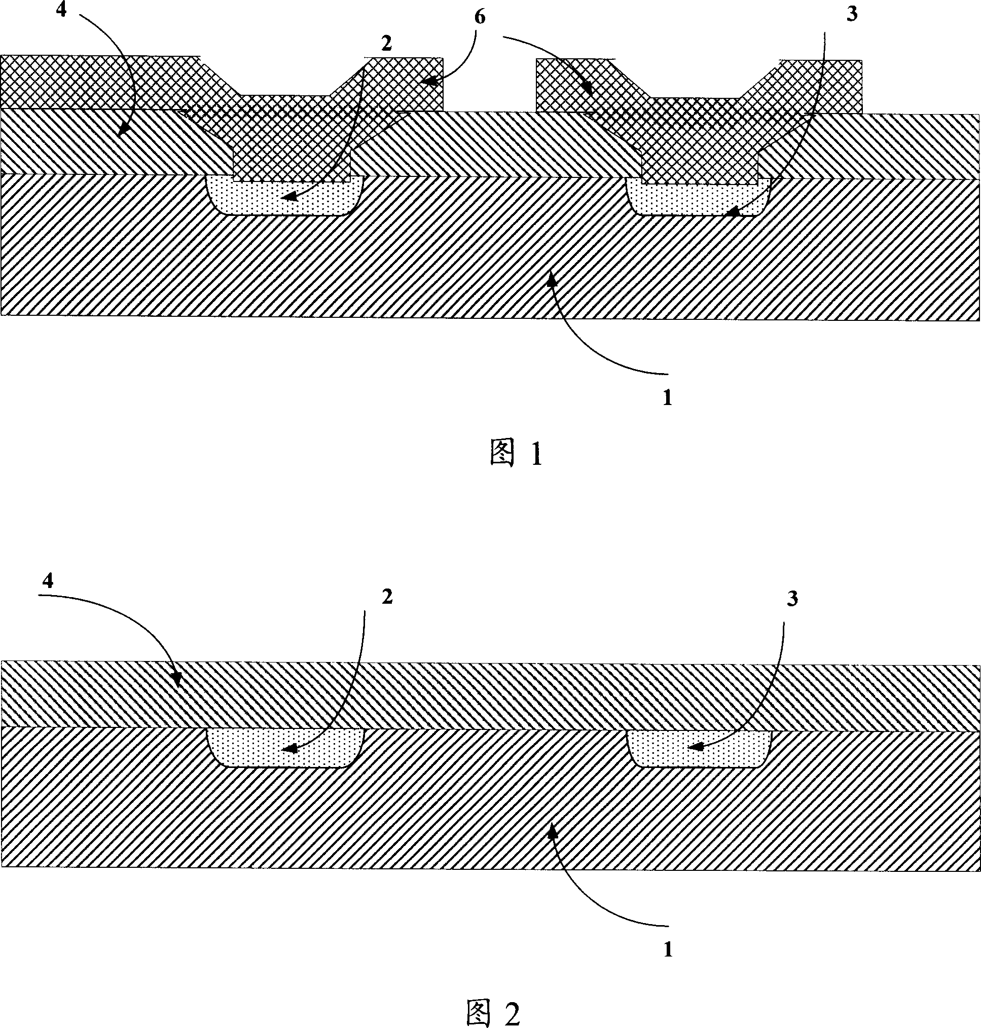
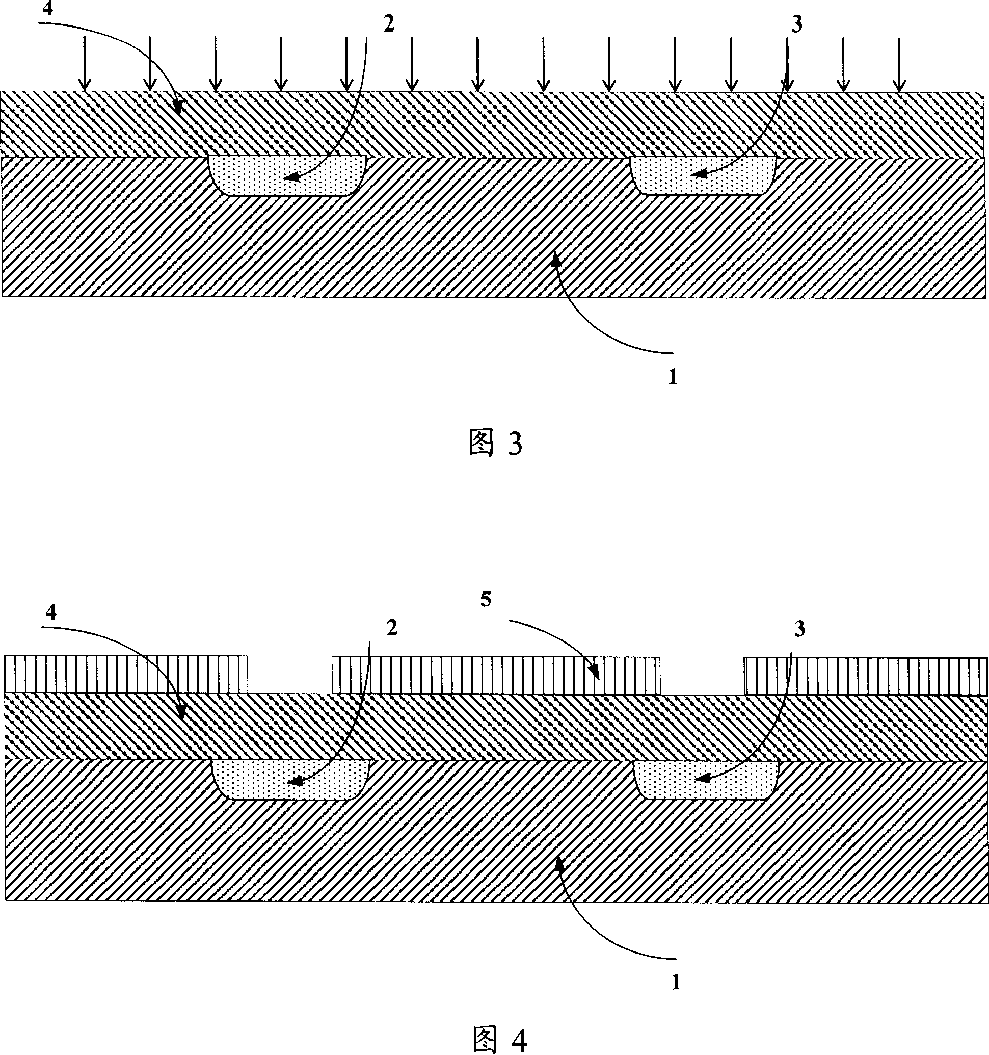
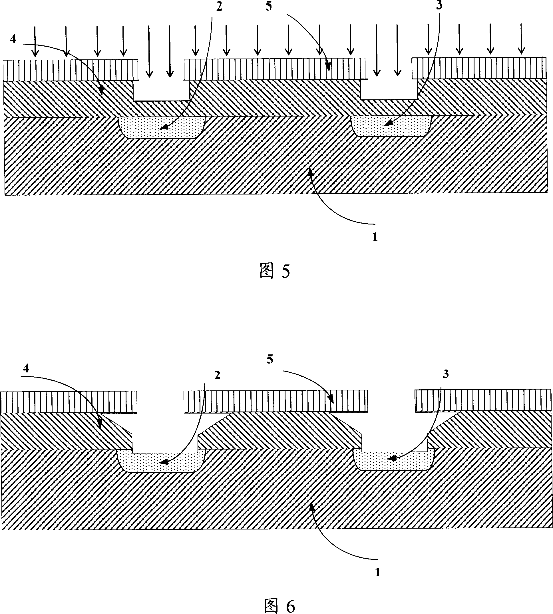
[0012] The invention provides a manufacturing process of a contact hole in an integrated circuit bipolar circuit, which can improve the shape of the contact hole without expensive advanced dry etching equipment. In the present invention, dry etching equipment is used to generate plasma before the contact hole is photolithographically coated. Since the dry etching equipment generates plasma to bombard the surface of silicon dioxide, the silicon dioxide becomes loose after the plasma bombardment, and in the next etching process, the rate will be accelerated, so it can be formed on the top of the contact hole. A good slope is formed, while the size of the contact hole remains unchanged; in addition, by adjusting the power of the plasma, the actual needs of different devices can be met, so that the shape of the contact hole can be adjusted. The details of the present invention will be disclosed in more detail below in conjunction with the accompanying drawings.
[0013] Please re...
PUM
 Abstract
Description
Claims
Application Information
 - R&D Engineer
- R&D Manager
- IP Professional
- Industry Leading Data Capabilities
- Powerful AI technology
- Patent DNA Extraction
Browse by: Latest US Patents, China's latest patents, Technical Efficacy Thesaurus, Application Domain, Technology Topic, Popular Technical Reports.
© 2024 PatSnap. All rights reserved.Legal|Privacy policy|Modern Slavery Act Transparency Statement|Sitemap|About US| Contact US: help@patsnap.com