Thin film transistor and manufacturing method thereof, display apparatus, method for modifying oxide film, method for forming oxide film, semiconductor device, method for manufacturing semiconductor d
A technology for thin film transistors and manufacturing methods, which is applied in the manufacture of semiconductor/solid-state devices, transistors, electrical components, etc., and can solve the problems of forming a uniform oxide film on difficult and complex surfaces, deterioration of film quality, and leakage current.
- Summary
- Abstract
- Description
- Claims
- Application Information
AI Technical Summary
Problems solved by technology
Method used
Image


Examples
no. 1 Embodiment approach
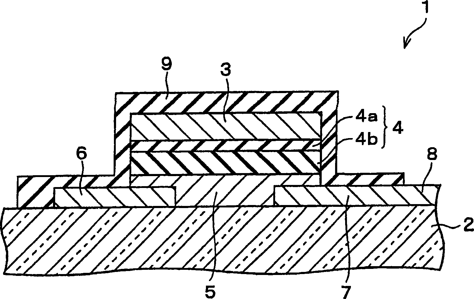
[0149] The following is based on Figure 1 to Figure 20 Embodiments of the present invention will be described. However, the present invention is not limited thereto.
[0150] Embodiments of the present invention will be described below by taking a thin film transistor (TFT) applied to a flexible liquid crystal display or an IC as an example. The manufacturing method (this manufacturing method) of the thin film transistor of the present invention is a kind of substrate that will form gate oxide film (chemical oxide film) be dipped in the solution that contains active oxidation species, directly oxidize this substrate surface, thereby form High-quality oxide film method.
[0151] First, problems in the manufacture of TFTs used in flexible liquid crystal displays, ICs, and the like will be described.
[0152]In order to manufacture flexible liquid crystal displays and the like, it is necessary to form TFTs on organic substrates such as PET. This organic substrate has a low m...
manufacture example 1
[0228] The following describes the formation of SiO with a film thickness of 3.5 nm by two-stage solution oxidation to form a chemical oxide film. 2 condition of the membrane.
[0229] First, in order to form the first chemical oxide film (silicon dioxide film 41), the substrate 2 to be processed is immersed in a 40% (wt) nitric acid aqueous solution without applying a voltage to form a porous film with a thickness of 1.1 nm. , The atomic density of the relatively low atomic density is 2.22×10 22 atom / cm 3 SiO 2 film (first oxide film 4a; chemical oxide film) 41 .
[0230] Next, in order to form the second chemical oxide film, the substrate on which the silicon dioxide film 41 has been formed remains immersed in the above-mentioned 40% (wt) nitric acid aqueous solution, and heated to an azeotropic nitric acid solution with a nitric acid concentration of 68% (wt). Aqueous solution (boiling point: 120.7°C), forming a thicker than the first chemical oxide film with an atomic ...
manufacture example 2
[0240] A second manufacturing example of the present invention will be described. In the case of forming a TFT using polysilicon on a substrate, a laminated silicon dioxide film (SiO 2 ). Therefore, in the example (manufacturing example 2) described here also, a silicon dioxide film is formed on polysilicon on the substrate (ie, the silicon substrate 11 is a polysilicon substrate) to manufacture a MOS capacitor (capacitance insulating film thereof).
[0241] In this case, silicon dioxide (SiO 2 )membrane.
[0242] Same as above-mentioned manufacturing example 1 (refer to Figure 2(a) to Figure 2(f) ), firstly, in order to form the first chemical oxide film, the polysilicon layer on the substrate was dipped into 40% (wt) nitric acid aqueous solution (making it contact) under the state of no voltage applied, forming a SiO layer with a thickness of 1.1 nm. 2 film (chemical oxide film) 41 (FIG. 2(c)).
[0243] Next, in order to form the second chemical oxide film, the above-m...
PUM
| Property | Measurement | Unit |
|---|---|---|
| Film thickness | aaaaa | aaaaa |
| Thickness | aaaaa | aaaaa |
| Leakage current density | aaaaa | aaaaa |
Abstract
Description
Claims
Application Information
 - Generate Ideas
- Intellectual Property
- Life Sciences
- Materials
- Tech Scout
- Unparalleled Data Quality
- Higher Quality Content
- 60% Fewer Hallucinations
Browse by: Latest US Patents, China's latest patents, Technical Efficacy Thesaurus, Application Domain, Technology Topic, Popular Technical Reports.
© 2025 PatSnap. All rights reserved.Legal|Privacy policy|Modern Slavery Act Transparency Statement|Sitemap|About US| Contact US: help@patsnap.com