DRAM chip device and multi-chip package comprising such a device

A technology of equipment and memory chips, applied in static memory, instruments, electrical digital data processing, etc.

Inactive Publication Date: 2006-12-27
秦蒙达股份公司
View PDF1 Cites 24 Cited by
  • Summary
  • Abstract
  • Description
  • Claims
  • Application Information

AI Technical Summary

Problems solved by technology

However, according to this proposal, a method of dealing with speed differences and operating different memory components in an efficient cost and time is not proposed

Method used


Image

  • DRAM chip device and multi-chip package comprising such a device
  • DRAM chip device and multi-chip package comprising such a device
  • DRAM chip device and multi-chip package comprising such a device

Examples


Embodiment Construction

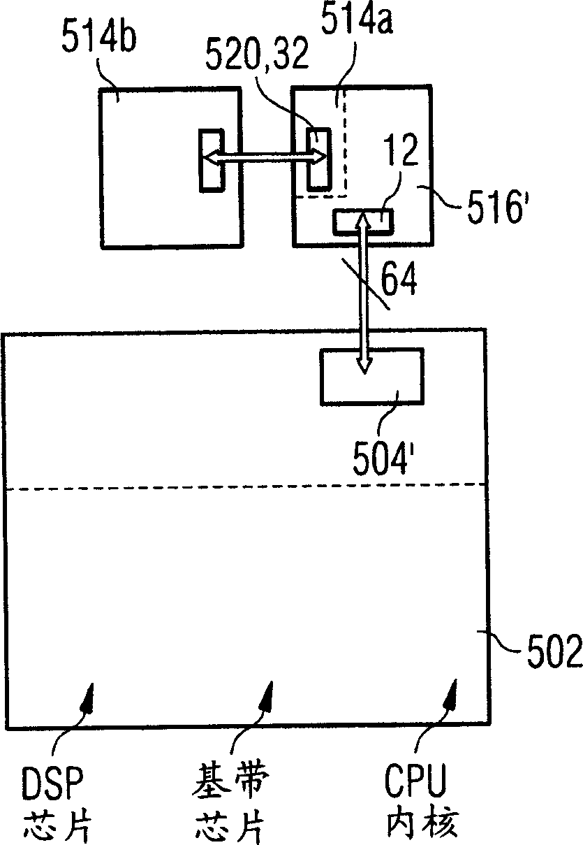
[0041] figure 2 An overall block diagram of the system according to the first embodiment of the present invention is shown. The system includes a CPU 502, an SDRAM working memory 516', and a NAND flash memory 514b for permanent storage of user data and executable program files. The CPU 502 has a single (first) interface 504' that provides communication with the volatile working memory 516' and the non-volatile memory 514b. Compared with the 60 lines or pins shown in the prior art example shown in FIG. 1, the width of this bus is increased to 64 data, command and address lines, or pins on the corresponding memory chip device.

[0042] However, since the interface 504' is the only interface reserved on the CPU side, the total number of wires or pads required on the CPU board 502 is reduced from 131 to 64 according to this specific example. The flash memory 514b is accessed from the SDRAM working memory 516' through the second interface 520. More precisely, the SDRAM working memory...


PUM


Abstract

An SDRAM memory chip device comprises a non-volatile memory controller for operating a non-volatile memory, e.g., a NAND-flash, and a FIFO memory buffer. The FIFO memory buffer serves to operate background store and load operations between a FIFO buffer array and the non-volatile memory, while a host system such as a CPU exchanges data with the SDRAM work memory. The SDRAM memory chip device, therefore, has at least two additional pins as compared with conventional SDRAM standard for generating a set of additional commands. These commands are employed by the FIFO memory buffer to manage the data transfer between the FIFO buffer and each of the non-volatile memory and the volatile SDRAM memory. Two further pins reflecting the flash memory status provide appropriate issuance of load or store signals by the host system.

Description

Technical field [0001] The present invention relates to a DRAM memory chip device and further relates to a multi-chip package (MCP) including such a device. The invention further relates to a flash memory device and a flash memory controller for controlling the operation of such a device. The invention further relates to associating working memory and data storage memory with CPUs used in mobile systems such as digital cameras and cellular phones. Background technique [0002] Recently, mobile systems such as cellular phones or digital cameras have made considerable improvements in their system logic and related memory. According to the specific requirements for such a system, many memory types are now included in the mobile system at the same time. [0003] For example, cellular phones and digital cameras have system logic that includes many chips that perform specific tasks related to mobile systems. For example, a cellular phone has a baseband chip for performing wireless comm...

Claims


Application Information

Patent Timeline
Patent Type & Authority Applications(China)
IPC IPC(8): G06F12/00
CPCG11C7/10G06F13/1673G11C11/4093
Inventor Y·福库佐
Owner 秦蒙达股份公司
Why Eureka
Try Eureka