Voltage level conversion circuit

A technology for transforming circuits and voltage levels, which is applied in logic circuit connection/interface layout, electrical components, electronic switches, etc. It can solve problems such as low threshold value, difficult to withstand high-voltage series transistors, and obstacles to miniaturization of low-power transistors. , to achieve the effect of high speed

Inactive Publication Date: 2005-11-23
PANASONIC CORP
View PDF1 Cites 3 Cited by
  • Summary
  • Abstract
  • Description
  • Claims
  • Application Information

AI Technical Summary

Problems solved by technology

[0024] As mentioned above, in Image 6 In the conventional voltage level conversion circuit 201 composed of two-stage negation circuits shown, since the subsequent negation circuit using the low power supply voltage VDD2 as the power supply voltage is composed of VDD1 withstand voltage series (high voltage series) transistors, the transistor's The threshold voltage is high, and it is difficult to operate this high-voltage series transistor with a low power supply voltage lower than the threshold voltage
Therefore, there is a problem that such a voltage level conversion circuit 201 constitutes a factor that prevents the reduction of power consumption by low-voltage driving in semiconductor devices or the miniaturization of transistors.
[0025] in addition, Figure 7 The illustrated level shifting circuit 202, as described above, is considered to be a circuit that converts a logic voltage level corresponding to a low power supply voltage to a logic voltage level corresponding to a high power supply voltage. In the case where the circuit structure is applied to a voltage level conversion circuit that converts a logic voltage level corresponding to a high power supply voltage into a logic voltage level corresponding to a low power supply voltage, the transistor 13 that applies a logic voltage corresponding to a high power supply voltage It is a high-voltage transistor with a thick gate oxide film, so there is a problem that the threshold value of a transistor with a low power supply voltage cannot be lower than that of a transistor with a high power supply voltage as a withstand voltage

Method used


Image

  • Voltage level conversion circuit
  • Voltage level conversion circuit
  • Voltage level conversion circuit

Examples


Embodiment approach 1

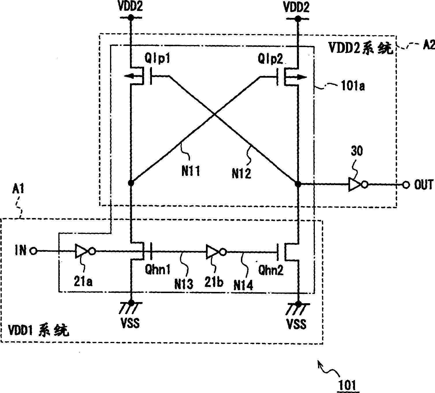
[0046] figure 1 It is a circuit diagram illustrating a voltage level conversion circuit according to Embodiment 1 of the present invention.

[0047] The voltage level conversion circuit 101 of the first embodiment converts an input signal having a logic voltage level of a high power supply voltage system (VDD1 system) into an output signal having a logic voltage level of a low power supply voltage system (VDD2 system) output circuit. This voltage level conversion circuit 101 is composed of a high-voltage resistant N-channel MOS transistor and a low-voltage resistant P-channel MOS transistor whose threshold value is lower than that of the transistor, and has a system of inputting VDD1 only to the gate of the high-voltage resistant N-channel MOS transistor. The input signal level shifter outputs the input signal level-shifted by the level shifter to a circuit driven by a low power supply voltage, so that the power supply voltage of the VDD2 system can be lowered.

[0048] f...

Embodiment approach 2

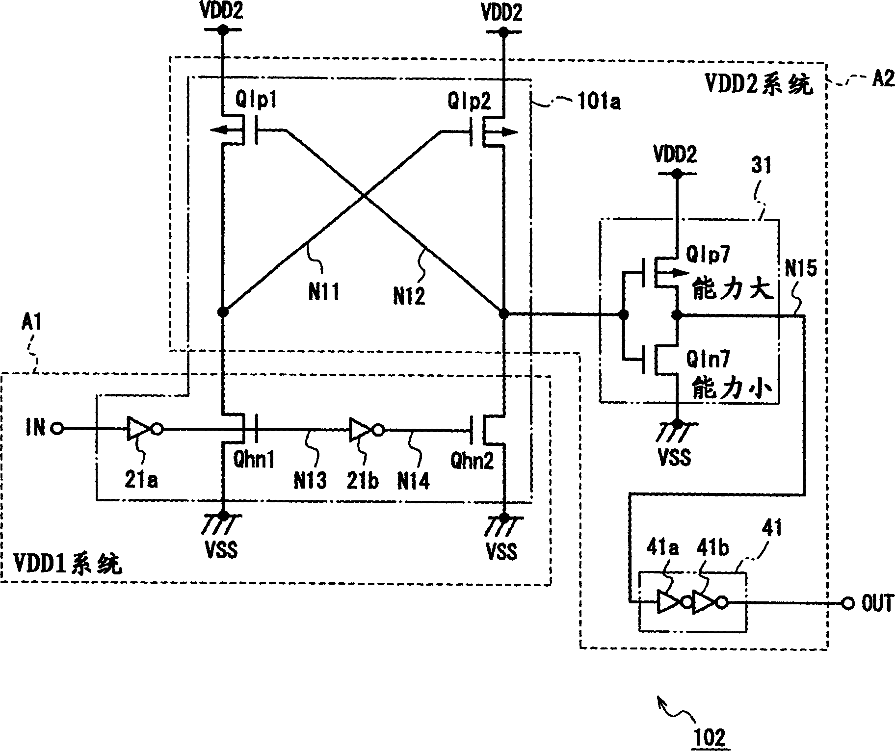
[0059] figure 2 It is a circuit diagram illustrating a voltage level conversion circuit according to Embodiment 2 of the present invention.

[0060] The voltage level conversion circuit 102 of the second embodiment has a negation circuit 31 for adjusting the balance of transistor capabilities in the level conversion unit 101a instead of the negation circuit 30 of the voltage level conversion circuit of the first embodiment. The output circuit 41 outputs the output signal of the negation circuit 31.

[0061] figure 2 Among them, the voltage level conversion circuit 102 has a level conversion unit 101a having the same configuration as that of the first embodiment, a negation circuit 31 for inverting a signal output from the level conversion unit 101a, and a “NEGAT” output to the negation circuit 31. The output circuit 41 that outputs the "signal after waveform shaping. The negation circuit 31 is composed of a third P-channel MOS transistor Q1p7 and a third N-channel MOS tra...

Embodiment approach 3

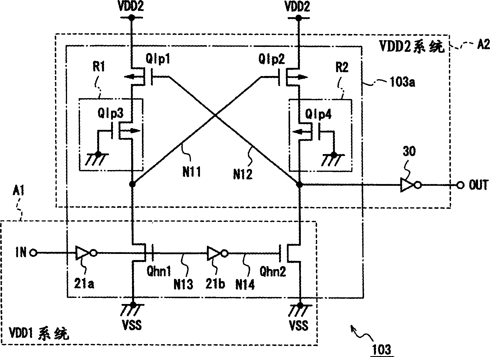
[0071] image 3 It is a circuit diagram illustrating a voltage level conversion circuit according to Embodiment 3 of the present invention.

[0072] The voltage level conversion circuit 103 of the third embodiment includes a level conversion unit 103a instead of the level conversion unit 101a of the voltage level conversion circuit of the first embodiment.

[0073] The level conversion unit 103a of the voltage level conversion circuit according to the third embodiment is configured by inserting a resistor R1 between the first connection node N11 of the level conversion unit 101a of the first embodiment and the first P-channel MOS transistor Q1p1. A resistor R2 is inserted between the second connection node N12 of the level conversion unit 101a and the second P-channel MOS transistor Q1p2.

[0074] Here, resistor R1 is composed of P-channel MOS transistor Q1p3 connected in series between first connection node N11 and first P-channel MOS transistor Q1p1, and having a gate conne...


PUM


Abstract

To make a voltage level converting circuit, which converts an input signal having a logical voltage level corresponding to a high power supply voltage VDD1 into a signal having a logical voltage level corresponding to a low supply voltage VDD2 and outputs it, operable at the lower low supply voltage VDD2. A power source level converting circuit comprises a level converting portion for converting an input signal of a VDD1 system to a signal of a VDD2 system and a NOT circuit 30 for reversing the level converted input signal and outputting it. Outputs of NOT circuits and of the VDD1 system constituting the level converting portion 101a are inputted only into high breakdown voltage transistors Qhn1 and Qhp2 in the level converting portion . A signal having a logical voltage level corresponding to the low supply voltage VDD2 is inputted in low breakdown voltage transistors Qln1 and Qlp2 in the level converting portion . Furthermore, only the level converted input signal from the level converting portion is inputted into the NOT circuit at post-stage of the level converting portion .

Description

technical field [0001] The present invention relates to a voltage level conversion circuit, in particular to converting an input signal having a logic voltage level corresponding to a first power supply voltage into a logic voltage level corresponding to a second power supply voltage lower than the first power supply voltage After the output signal is output, the voltage level conversion circuit is output. Background technique [0002] In recent years, with miniaturization of semiconductor devices, two types of voltages, an external voltage and an internal voltage, are used, and the internal voltage is set lower than the external voltage. Therefore, a circuit for converting the logic voltage level of a signal is required between a circuit driven by an external voltage and a circuit driven by an internal voltage. [0003] Hereinafter, conventional art will be described with respect to a circuit (hereinafter referred to as a voltage level conversion circuit) that converts a l...

Claims


Application Information

Patent Timeline
Patent Type & Authority Applications(China)
IPC IPC(8): H03K19/0185H03K3/012H03K3/356H03K17/10H03L5/00
CPCH03K3/356165H03K17/102H03K3/012H03K3/356113
Inventor 平野博茂
Owner PANASONIC CORP
Why Eureka
Try Eureka