Bias voltage applying circuit and semiconductor memory device

一种偏置电压、偏置电路的技术,应用在读出技术领域,能够解决导通电阻变高、阻碍高速读出、过渡特性恶化等问题,达到高增益、实现高速读出的效果

Inactive Publication Date: 2005-08-17
SHARP KK
View PDF1 Cites 9 Cited by
  • Summary
  • Abstract
  • Description
  • Claims
  • Application Information

AI Technical Summary

Problems solved by technology

[0009] However, in Figure 9 In the bias voltage applying circuit of the conventional example 2 shown, since an additional stage of the select transistor 200 is required for switching the left and right bit lines, and an additional resistance component is added to the memory cell current path, the bit The CR (capacitance-resistance product) of the line increases and the transition characteristics deteriorate, becoming the main factor hindering high-speed readout
[0010] In addition, in Figure 10 In the bias voltage applying circuit of the conventional example 3 shown, the Vds (voltage between the drain and the source) of the PMOS switching transistor 300 is approximately 0V, so the on-resistance thereof becomes high, and the PMOS voltage of the load circuit 103 It takes time before the gate potential becomes equal to the drain potential
Therefore, in the meantime, since the current mirror does not work properly, it becomes a major factor hindering high-speed readout
[0011] In addition, the load circuit 103 of any of the bias voltage applying circuits of the conventional examples 2 and 3 is asymmetrical, so a difference is generated in the load capacitance of the input node of the sense amplifier of the next stage, and there is a transient response characteristic caused by the correlation Dangers that hinder high-speed readout from different

Method used


Image

  • Bias voltage applying circuit and semiconductor memory device
  • Bias voltage applying circuit and semiconductor memory device
  • Bias voltage applying circuit and semiconductor memory device

Examples


no. 1 approach

[0049] A first embodiment of a semiconductor memory device and a bias voltage applying circuit (hereinafter referred to as "the device of the present invention" and "the circuit of the present invention" as appropriate) according to the present invention will be described with reference to the drawings.

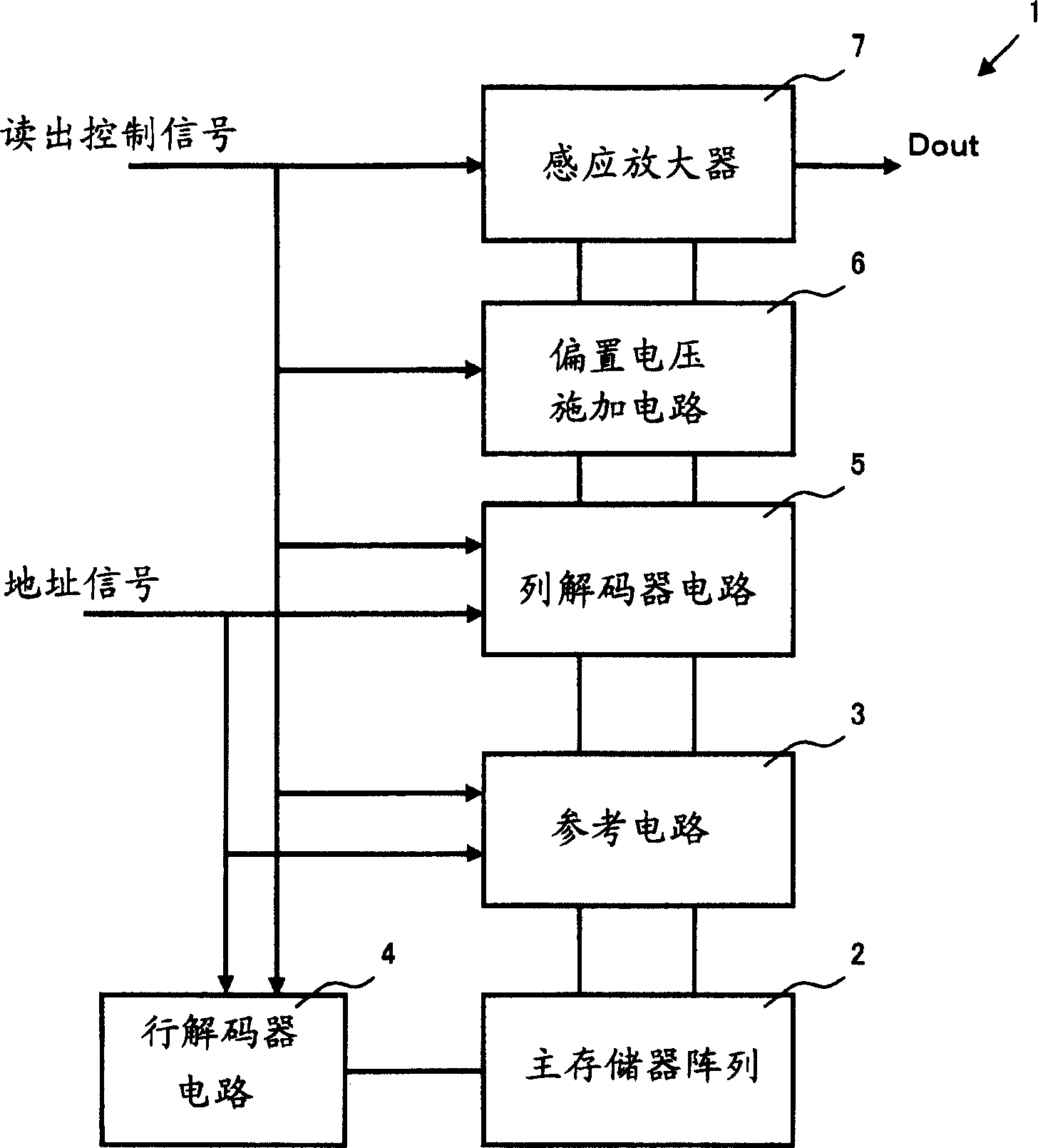
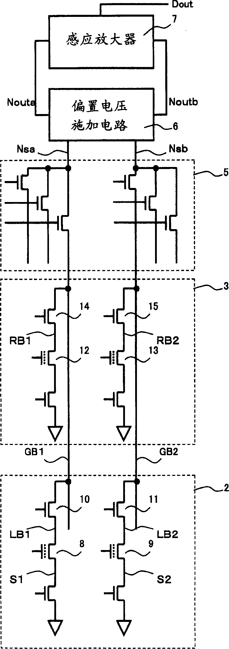
[0050] Such as figure 1 As shown, the device 1 of the present invention has: a main memory array 2, a reference circuit 3, a row decoder 4, a column decoder 5, a bias voltage applying circuit 6 involved in the present invention, a sense amplifier 7, and the like. Also, although not shown, necessary address signals and read control signals (chip enable signal, output enable signal, etc.) are separately supplied to each part via respective input circuits. In addition, the output Dout of the sense amplifier 7 is output to the outside via a predetermined output circuit.

[0051] The main memory array 2 is configured by arranging a plurality of memory cells to be read in an arra...

no. 2 approach

[0071] Next, the circuit configuration and circuit operation of the second embodiment of the semiconductor memory device according to the present invention will be described with reference to the drawings.

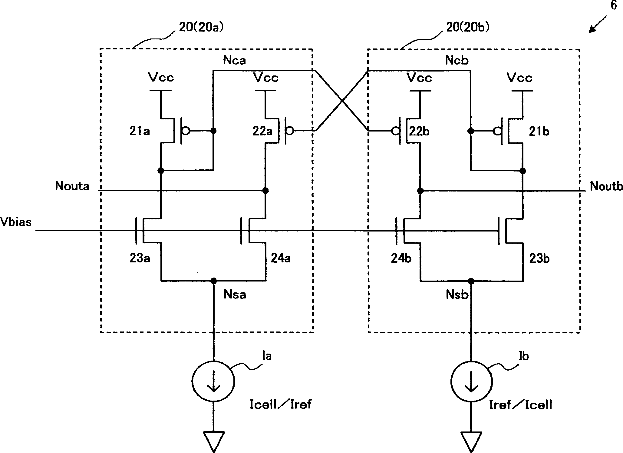
[0072] As shown in FIG. 11 , the inventive circuit 6 of this embodiment has two completely equivalent bias circuits 30 . As in the first embodiment, one is called a first bias circuit 30a, and the other is called a second bias circuit 30b. In addition, in the figure, the two current sources Ia and Ib are the same as those in the first embodiment, one of which represents the memory cell current Icell of the selected memory cell, and the other represents the reference cell current Iref of the reference memory cell. The memory cell current Icell of the selected memory cell varies according to the threshold voltage corresponding to the stored information.

[0073] The bias circuits 30a ( 30b ) of this embodiment are each composed of active elements including six MOSFETs. The...

no. 3 approach

[0084] Next, the circuit configuration and circuit operation of the third embodiment of the semiconductor memory device according to the present invention will be described with reference to the drawings. In the second embodiment, the current path is divided and the memory cell current Icell or the reference memory cell current Iref copied from the first active element to the third active element is used, but in this embodiment, the current path is not divided. , but copy the current from the first active element to the third active element and the fourth active element respectively.

[0085] As shown in FIG. 12 , the inventive circuit 6 of this embodiment has two completely equivalent bias circuits 40 . As in the first and second embodiments, one is called a first bias circuit 40a, and the other is called a second bias circuit 40b. In addition, in the figure, the two current sources Ia and Ib are the same as those in the first and second embodiments, one of which represents ...


PUM


Abstract

Two bias circuits (20) which supply a current to a selected memory cell and a reference memory cell have the same circuit constitution. Each bias circuit includes a first active element (21a, 21b) between a power supply node Vcc and a junction node (Nca, Ncb), where a current is controlled to prevent a voltage level at the junction node from fluctuating, a second active element (22a, 22b) between the power supply node and an output node (Nouta, Noutb), where a current is controlled such that a voltage level at the output node is changed in direction opposite to a voltage level at the junction node in other bias circuit, a third active element (23a, 23b) and a fourth active element (24a, 24b) between the junction node and a current supply node Nsa (Nsb) and between the output node and the current supply node, respectively, where a bias voltage is adjusted.

Description

technical field [0001] The present invention relates to a semiconductor memory device, and more specifically, to a readout technique for detecting a current flowing in a memory cell of the semiconductor memory device and determining its memory state at high speed. Background technique [0002] In a semiconductor memory device, various methods are used to read the memory state of its memory cells. A flash memory which is one of nonvolatile semiconductor memory devices will be described as an example. The flash memory is configured such that each memory cell has a memory transistor having a floating gate structure, and stores information based on the accumulated charge (electron) injected into the floating gate of each memory cell. Specifically, in a state where many electrons are injected into the floating gate, it is difficult to form an inversion layer in the channel region, so the threshold voltage of the memory cell becomes high (defined as a program ...

Claims


Application Information

Patent Timeline
Patent Type & Authority Applications(China)
IPC IPC(8): G11C16/06G11C7/06G11C7/12G11C16/28G11C29/02
CPCG11C2207/063G11C7/12G11C7/06G11C29/028G11C29/021G11C29/02G11C7/062G11C16/28G11C2029/5004G11C5/14
Inventor 森康通吉本贵彦渡边雅彦安西伸介野岛武正木宗孝
Owner SHARP KK
Why Eureka
Try Eureka