Wafer lens array forming method, forming die, and wafer lens array

A lens array, wafer-level technology, applied in the direction of lens, color TV parts, TV system parts, etc., to achieve the effect of suppressing dispersion

Inactive Publication Date: 2015-07-01
FUJIFILM CORP
View PDF47 Cites 0 Cited by
  • Summary
  • Abstract
  • Description
  • Claims
  • Application Information

AI Technical Summary

Problems solved by technology

[0016] However, when a resin is sandwiched between a pair of mold members, a part of the resin sometimes protrudes from the mold surface of the mold members to the outside of the mold member.

Method used


Image

  • Wafer lens array forming method, forming die, and wafer lens array
  • Wafer lens array forming method, forming die, and wafer lens array
  • Wafer lens array forming method, forming die, and wafer lens array

Examples


Embodiment Construction

[0052] Hereinafter, embodiments of the present invention will be described in detail based on the drawings.

[0053] First, the structure of the wafer-level lens array, lens module, and camera module will be described.

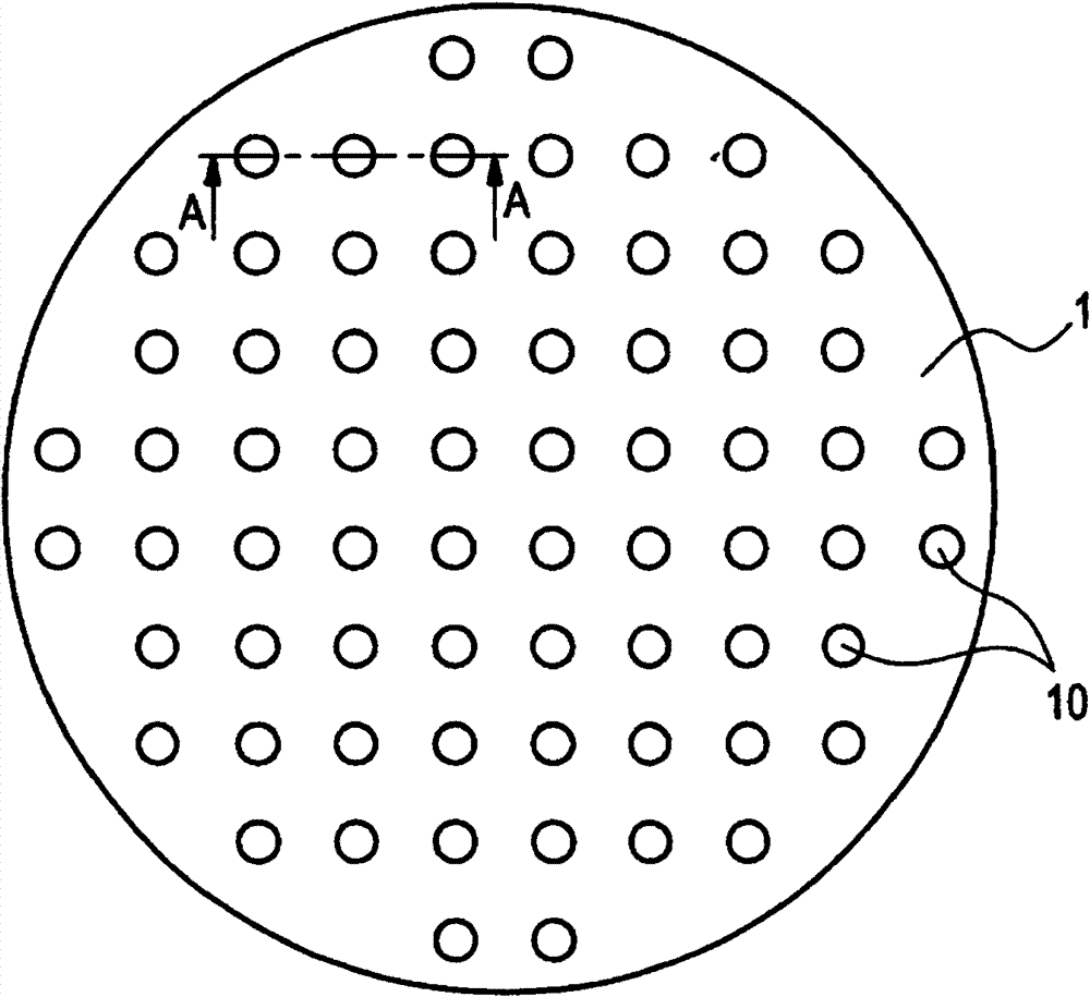
[0054] figure 1 is a top view of the wafer-level lens array. The wafer-level lens array has a substrate unit 1 and a plurality of lens units 10 arranged on the substrate unit 1 .

[0055] The lens unit 10 is made of the same material as the substrate unit 1 and is integrally formed on the substrate unit 1 .

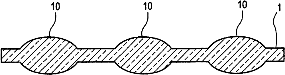
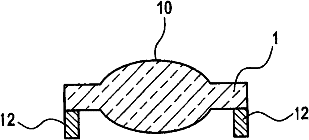
[0056] figure 2 yes figure 1 A-A cross-sectional view of the wafer-level lens array shown. The lens portion 10 formed on the substrate portion 1 has a convex lens shape having a convex surface protruding from a planar portion of the substrate portion 1 . The shape of the lens portion 10 is not particularly limited, and may be appropriately deformed depending on the application or the like.

[0057] A wafer-level lens array is obtained by molding...


PUM

PropertyMeasurementUnit
viscosityaaaaaaaaaa
particle sizeaaaaaaaaaa
Abbe numberaaaaaaaaaa

Abstract

The invention provides a forming method capable of preventing the position of a lens part of a manufactured wafer lens array from scattering and a forming die. The method for forming a wafer lens array having a substrate part and plural lens parts arranged on the substrate part has a first step of a measuring process in which a pair of die components is applied and an area distinguished by a dike part formed by enclosing the whole periphery of a die component along one die face is supplied with liquid resin which is used as the material of wafer lens array and meanwhile the redundant resin flows out from the area distinguished by the dike part. Therefore, the required resin to be applied in forming a wafer lens array is measured, wherein, the die faces comprises a lens transfer printing part making the shape of the lens part formed by counter-rotating. The method further comprises a deforming process in while the resin maintained in the area is clamped by the pair of the die components and then deformed in a die face shape; and a solidifying process in while the resin clamped by the pair of die components is solidified.

Description

technical field [0001] The invention relates to a forming method of a wafer-level lens array, a forming mold, a wafer-level lens array, a lens module and a camera assembly. Background technique [0002] In recent years, small and thin imaging modules have been mounted on portable terminals of electronic devices such as mobile phones and PDAs (Personal Digital Assistants). Such an imaging module generally includes a solid-state imaging element such as a CCD (Charge Coupled Device) image sensor or a CMOS (Complementary Metal-Oxide Semiconductor) image sensor, and a lens for forming a subject image on the solid-state imaging element. [0003] Along with miniaturization and thinning of portable terminals, miniaturization and thinning of imaging modules are required. In addition, in order to reduce the cost of portable terminals, it is desired to improve the efficiency of the manufacturing process. As a method of manufacturing a small number of lenses, there is known a method o...

Claims


Application Information

Patent Timeline
Patent Type & Authority Patents(China)
IPC IPC(8): B29C33/00G02B3/00H04N5/225B29D11/00B29L11/00
Inventor 榊毅史渡边清一
Owner FUJIFILM CORP
Why Eureka
Try Eureka