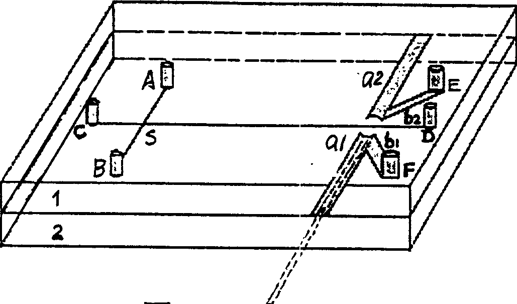
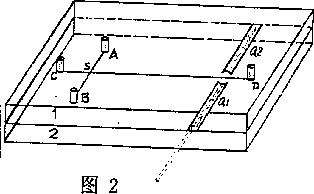
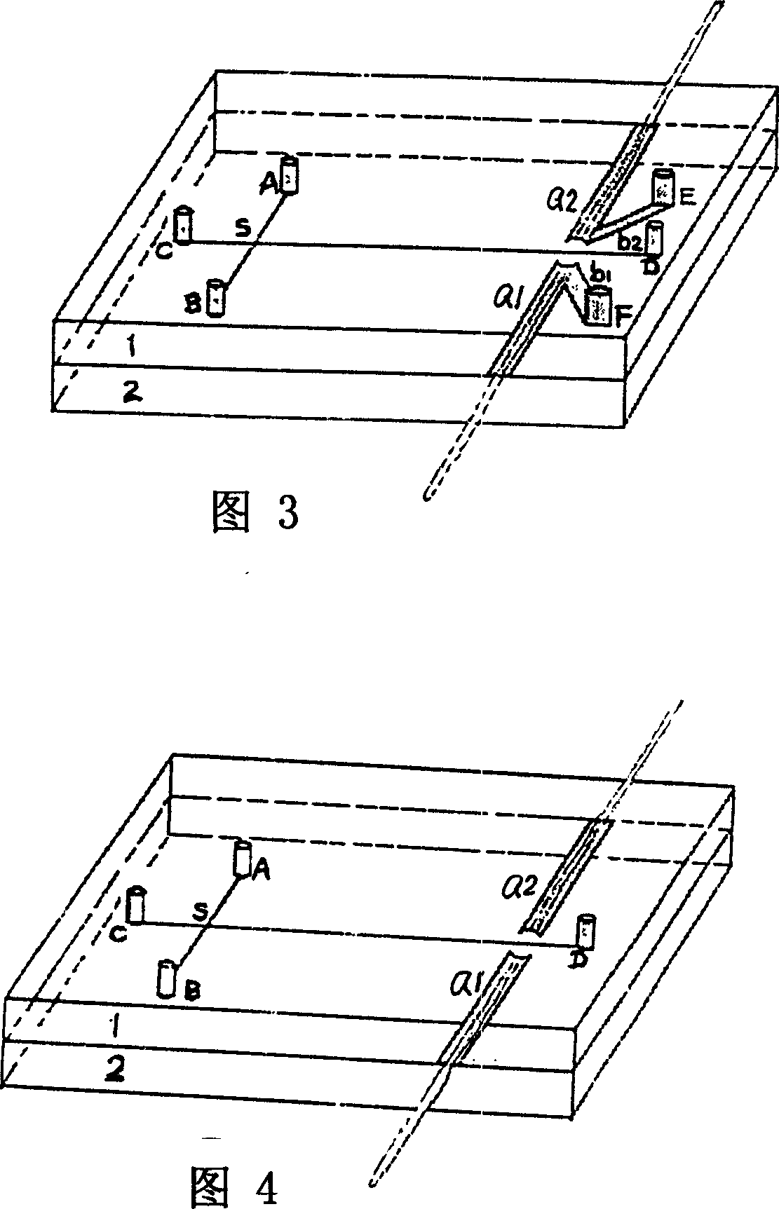
Laser induced fluorescence and light absorption bifunction detecting microflow controlled electrophoresis ehip
A laser-induced fluorescence and electrophoresis chip technology, which is applied in fluorescence/phosphorescence, color/spectral characteristic measurement, measurement devices, etc., can solve the problems of single function and complex structure of optical detection system, and achieves ingenious design and simple operation of optical path. , the effect of benefiting the resolution and detection sensitivity
- Summary
- Abstract
- Description
- Claims
- Application Information
AI Technical Summary
Problems solved by technology
Method used
Image

Examples
Embodiment 1
[0059] Example 1: Fabrication of fiber-coupled microfluidic electrophoresis chip made of glass
[0060] 1. Fabrication of chip substrate 2:
[0061] The size design of the microchannel on the mask film: the width of the fluid channel is 40 μm; the width of the fiber channel is 60 μm; the distance d between the fiber channel and the separation channel CD is 200 μm;
[0062] Place the mask film on a 63mm×63mm×1.5mm uniform chrome plate, expose to ultraviolet rays for 180 seconds (wavelength 365nm), develop in the developer for 100 seconds, and dry at 100°C for half an hour;
[0063] Corrode the chromium film with a chromium film etching solution (cerium sulfate: perchloric acid: water=50 grams: 15 milliliters: 300 milliliters) at room temperature, then rinse it with high-purity water, and dry it;
[0064] The channel size on the chromium plate was measured by digital microscope photography: the width of the fluid channel is 60 μm; the width of the optical fiber channel is 90 μm...
Embodiment 2
[0074] Example 2: Fabrication of PMMA laser-induced fluorescence and light absorption dual-function detection microfluidic electrophoresis chip
[0075] 1. Design of the glass positive template mask film (substrate and cover sheet): the width of the microfluidic channel on the positive template mask of the chip substrate is 120 μm; the width of the optical fiber channel on the positive template mask of the chip cover plate is 250 μm, The distance is 240 μm.
[0076] 2. Production of substrate positive template: place the chip substrate mask film on a 63mm×63mm×1.5mm uniform chrome plate, expose to ultraviolet rays for 5 minutes (wavelength 365nm), develop in the developer for 100 seconds, and bake at 100°C half an hour. The chromium film was etched with a chromium film etching solution (cerium sulfate: perchloric acid: water = 50 g: 15 ml: 300 ml) at room temperature, and then rinsed with water. With 0.2M HF / 0.2M NH 4 F etchant was used for etching, the rate was about 4 μm / ...
Embodiment 3
[0081] Example 3: Fabrication of a microfluidic electrophoresis chip for dual-function detection of laser-induced fluorescence and light absorption made of PDMS
[0082] 1. The design of the glass positive template mask film (substrate and cover sheet): the width of the microfluidic channel on the positive template mask of the substrate is 120 μm; the width of the optical fiber channel on the positive template mask of the cover plate is 250 μm, and the distance between the two optical fiber channels 240μm;
[0083] 2. Production of glass substrate positive template: place the substrate mask film on a uniform chrome plate of 63mm×63mm×1.5mm, expose to ultraviolet rays for 5 minutes (wavelength 365nm), develop in the developer for 100 seconds, and bake at 100°C half an hour. The chromium film was etched with a chromium film etching solution (cerium sulfate: perchloric acid: water = 50 g: 15 ml: 300 ml) at room temperature, and then rinsed with water. With 0.2M HF / 0.2M NH 4 F ...
PUM
| Property | Measurement | Unit |
|---|---|---|
| Bottom width | aaaaa | aaaaa |
| Bottom width | aaaaa | aaaaa |
| Depth | aaaaa | aaaaa |
Abstract
Description
Claims
Application Information
 - R&D
- Intellectual Property
- Life Sciences
- Materials
- Tech Scout
- Unparalleled Data Quality
- Higher Quality Content
- 60% Fewer Hallucinations
Browse by: Latest US Patents, China's latest patents, Technical Efficacy Thesaurus, Application Domain, Technology Topic, Popular Technical Reports.
© 2025 PatSnap. All rights reserved.Legal|Privacy policy|Modern Slavery Act Transparency Statement|Sitemap|About US| Contact US: help@patsnap.com