


Quick Research
Generate reliable direction feasibility study reports for your R&D in just a few steps.

Technical Q&A
Discover and master advanced knowledge NOW. Basics, ideas, possibilities, all at once.

Find Solutions
As an expert in R&D theories, this can generate solutions to your technical problems instantly.

Evaluate Feasibility
Analyze your overall solution with one click, know your potential R&D risks in advance.

Monitor Landscape
Get weekly tech updates, stay abreast of the latest tech innovations and key insights.
Semiconductor storage device and semiconductor integrated circuit device
A technology for storage devices and integrated circuits, applied in semiconductor devices, semiconductor/solid-state device manufacturing, logic circuit connection/interface layout, etc., can solve the problems of increasing the area of LSI chips and complex circuits, etc.
- Summary
- Abstract
- Description
- Claims
- Application Information
AI Technical Summary
Problems solved by technology
Method used
Image

Examples
no. 1 Embodiment approach
[0090] Hereinafter, the semiconductor memory device according to the first embodiment of the present invention will be described with reference to the drawings.
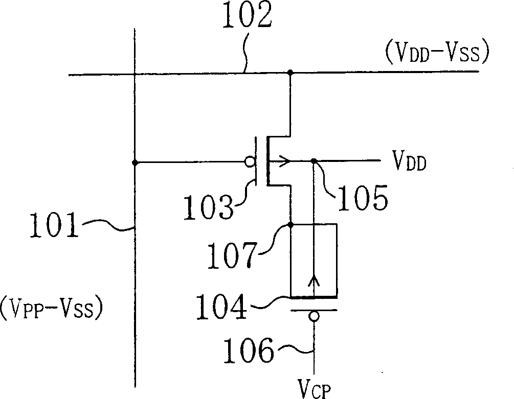
[0091] figure 1 It is a circuit diagram showing a memory cell in the dynamic semiconductor memory device (DRAM) according to the first embodiment of the present invention.
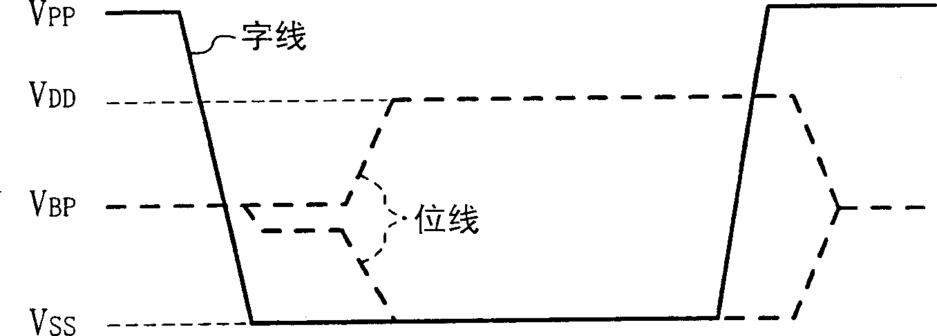
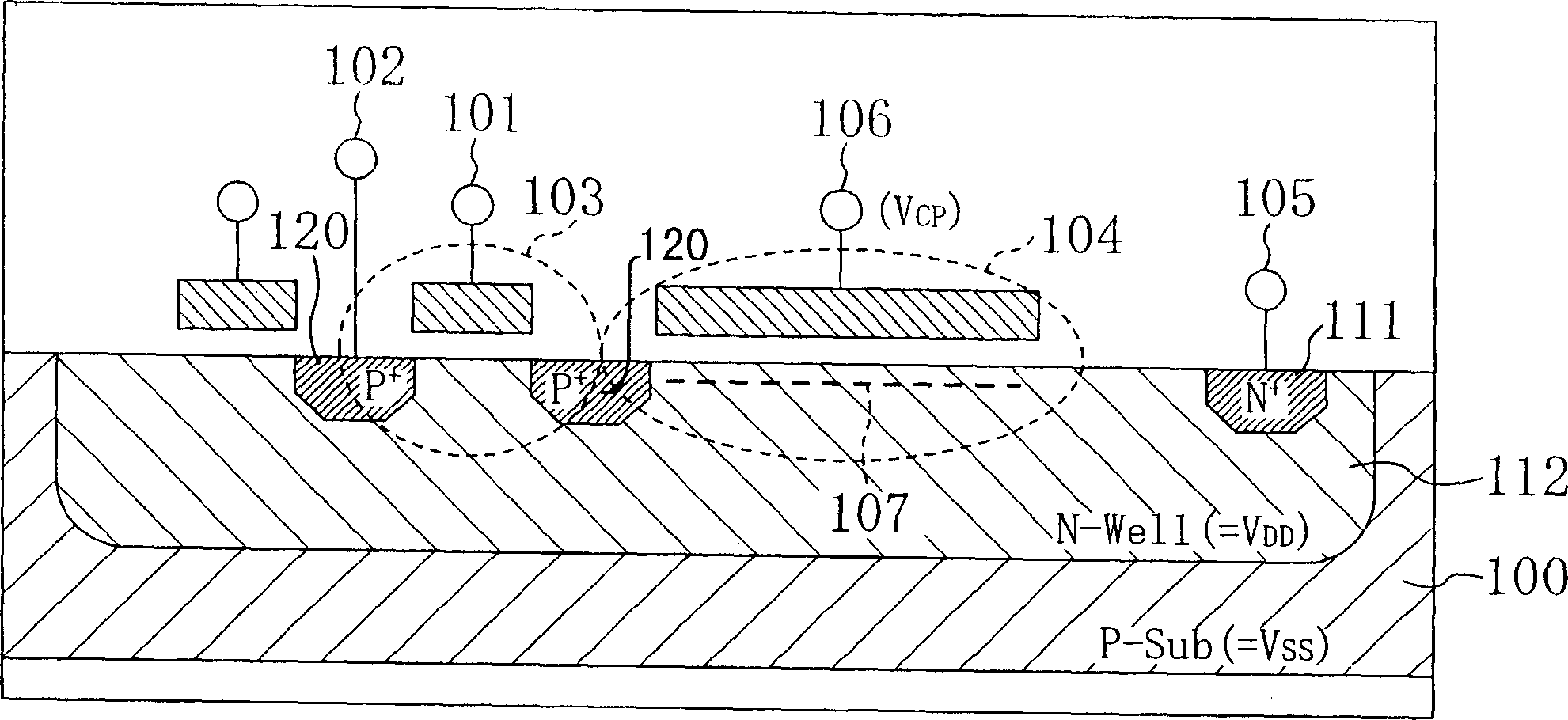
[0092] As shown in the figure, the DRAM of this embodiment includes: a plurality of word lines 101 and a plurality of bit lines 102 crossing each other; In addition, each memory cell includes: an access transistor (access Tr) 103 of a p-channel MOSFET whose gate electrode is connected to the word line 101 and one end (the first diffusion layer) is connected to the bit line 102; The other end (the second diffusion layer) is connected to the cell capacitor 104 of the p-channel MOSFET which functions as a capacitor. According to this configuration, in the DRAM of this embodiment, the memory cell storage node 107 between the access Tr 103 and the ...
no. 2 Embodiment approach
[0160] As a DRAM according to the second embodiment of the present invention, an example in which an access Tr of a memory cell and a cell capacitor are formed in common using n-channel MOSFETs will be described.
[0161] Figure 11 It is a circuit diagram showing a memory cell in the DRAM according to the second embodiment.
[0162] As shown in the figure, the DRAM of this embodiment includes: a plurality of word lines 121 and a plurality of bit lines 122 crossing each other; In addition, each memory cell includes: an access Tr123 of an n-channel MOSFET whose gate electrode is connected to the word line 121 and whose one end (the first diffusion layer) is connected to the bit line 122; and the other end of the access Tr123 ( The second diffusion layer) is a cell capacitor 124 that functions as a capacitor of the n-channel MOSFET connected. Like the first embodiment, the DRAM of this embodiment is provided on the same chip as the logic circuit and formed by logic processing....
PUM
 Abstract
Description
Claims
Application Information
 - R&D Engineer
- R&D Manager
- IP Professional
- Industry Leading Data Capabilities
- Powerful AI technology
- Patent DNA Extraction
Browse by: Latest US Patents, China's latest patents, Technical Efficacy Thesaurus, Application Domain, Technology Topic, Popular Technical Reports.
© 2024 PatSnap. All rights reserved.Legal|Privacy policy|Modern Slavery Act Transparency Statement|Sitemap|About US| Contact US: help@patsnap.com