Quick electrochemical electrode activating method
An activation method and electrochemical technology, which can be used in electrochemical variables of materials, scientific instruments, material analysis by electromagnetic means, etc., and can solve problems such as time-consuming and chip damage.
- Summary
- Abstract
- Description
- Claims
- Application Information
AI Technical Summary
Problems solved by technology
Method used
Image
Examples
Embodiment 1
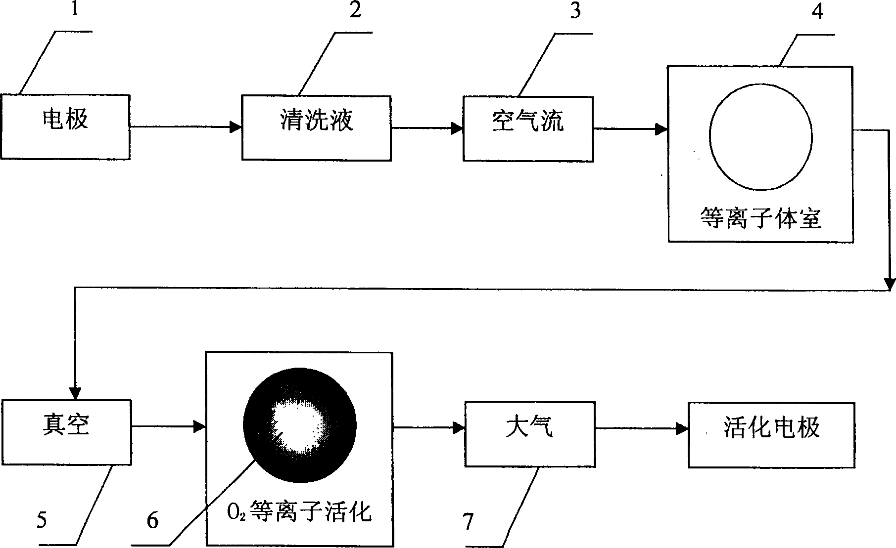
[0018] Example 1: figure 1 A flow block diagram showing the activation method of the electrochemical electrode 1 (thin film or thick film electrode 1a or electrode probe 1b) according to the embodiment of the present invention. This flow chart is used to explain the implementation of the present invention, not limited to describing the structure and parameters of the system / device. The quick activation method of the electrochemical electrode 1 is as follows: (1) Pre-cleaning: Rinse the surface of the electrode 1 with deionized water or ethanol cleaning solution 2, and dry it with the air flow 3 in the air gun to obtain a dry microelectrode 1; (2) Lofting: Put the electrode 1 into the plasma chamber 4, turn on the cooling water; (3) activation: turn on the power supply, and evacuate the plasma chamber 4 into a vacuum of 5 to 2×10 -2 Torr, the oxygen flow rate is set to 2L / min, the nitrogen pressure is 5psi, the radio frequency power is 70W, the base phase pressure is 30mTorr, ...
Embodiment 2
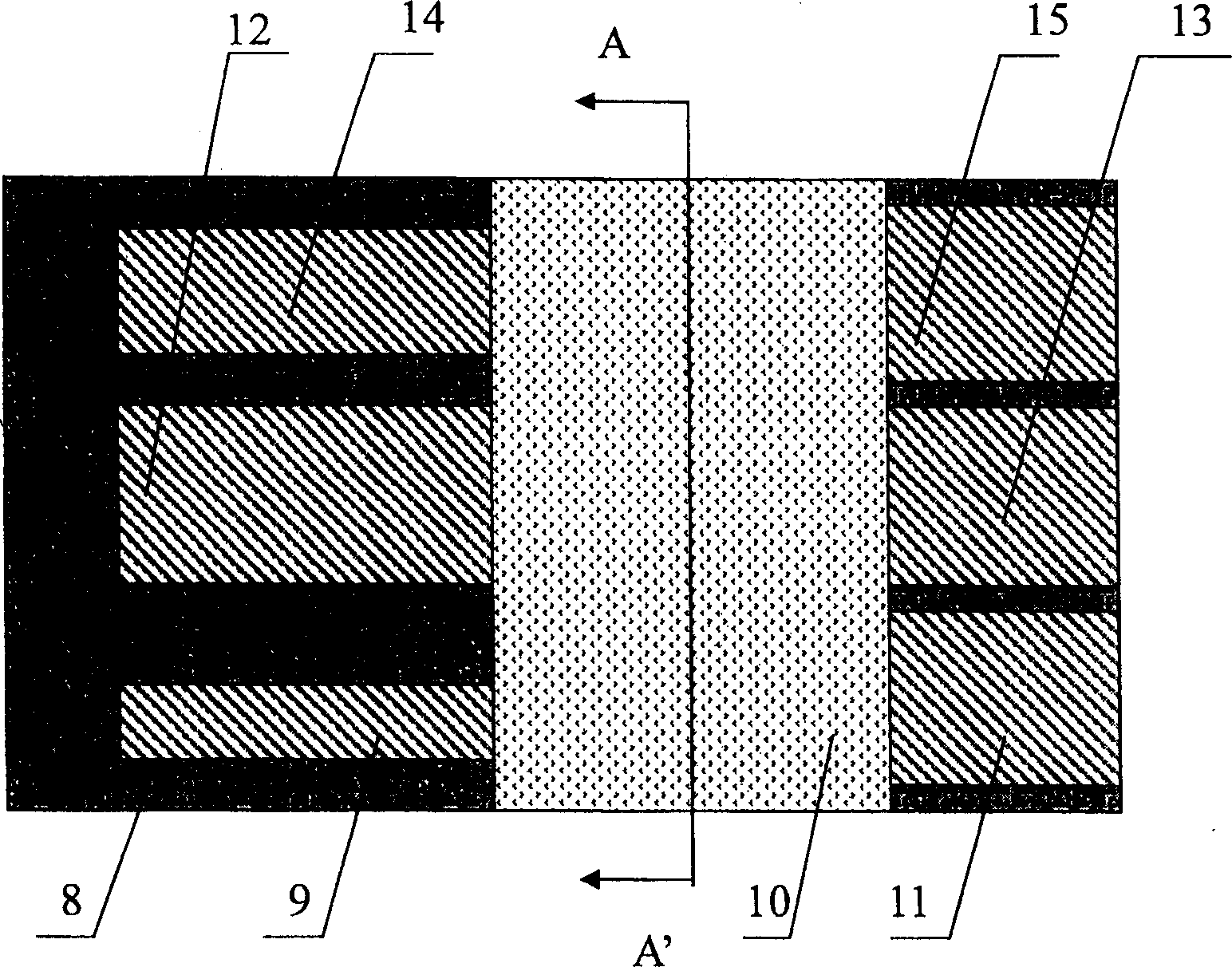
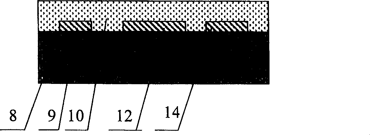
[0019] Example 2: figure 2 is a schematic diagram of a thin film or thick film electrode 1a activated using the present invention, image 3 yes figure 2 In the cross-sectional view of A-A', the thin film or thick film electrode 1a mainly includes the following parts: insulating material substrate 8, working electrode 9, insulating film 10, external plugging point or welding point 11 of the working electrode, counter electrode 12, counter electrode External plug points or welding points 13, reference electrode 14, external plug points or welding points 15 of the reference electrode. According to the present invention, according to figure 1 The steps shown activate the deactivated micro-film planar electrodes, Figure 4 It shows the comparison of the cyclic voltammogram before and after the rapid activation of the electrode. Before the activation, the surface of the electrode was polluted and deactivated, and the cyclic voltammogram i was flat. After activation, the surface...
Embodiment 3
[0020] Embodiment 3: according to the present invention, according to figure 1 The step shown activates the microelectrodes modified with platinum black particles on the surface of the deactivated thin film electrodes, Figure 5 It is a comparison of the cyclic voltammograms before and after the rapid activation of the electrode. Before the activation, the surface of the electrode was seriously polluted and deactivated, and its cyclic voltammogram i was flat without step changes. After activation, the surface of the electrode 1a was cleaned and activated, and its cyclic voltammogram ii was restored. Normal, the current output increased; the repeatability of the response after activation was tested and analyzed, and the half-wave potential in the cyclic voltammetry response after 8 activations was constant at 0.26V, and the mean peak value (Mean) of the oxidation current was 18nA. The standard deviation (Std.Dev) is 3nA, and the standard error (Std.Err) is 1nA, indicating that ...
PUM
 Abstract
Description
Claims
Application Information
 - R&D Engineer
- R&D Manager
- IP Professional
- Industry Leading Data Capabilities
- Powerful AI technology
- Patent DNA Extraction
Browse by: Latest US Patents, China's latest patents, Technical Efficacy Thesaurus, Application Domain, Technology Topic, Popular Technical Reports.
© 2024 PatSnap. All rights reserved.Legal|Privacy policy|Modern Slavery Act Transparency Statement|Sitemap|About US| Contact US: help@patsnap.com


