
Low-k interconnect structure comprised of a multilayer of spin-on porous dielectrics

A technology of interconnection structure and dielectric, applied in the direction of circuits, electrical components, electrical solid devices, etc., can solve the problems of increasing equipment purchase and maintenance costs, and achieve the effect of increasing production costs

Inactive Publication Date: 2004-06-16
GLOBALFOUNDRIES INC
View PDF0 Cites 16 Cited by
  • Summary
  • Abstract
  • Description
  • Claims
  • Application Information

AI Technical Summary

Problems solved by technology

The use of mixed tool sets increases the cost of equipment acquisition and maintenance, as well as the original time of manufacture

Method used


Image

  • Low-k interconnect structure comprised of a multilayer of spin-on porous dielectrics
  • Low-k interconnect structure comprised of a multilayer of spin-on porous dielectrics
  • Low-k interconnect structure comprised of a multilayer of spin-on porous dielectrics

Examples


example

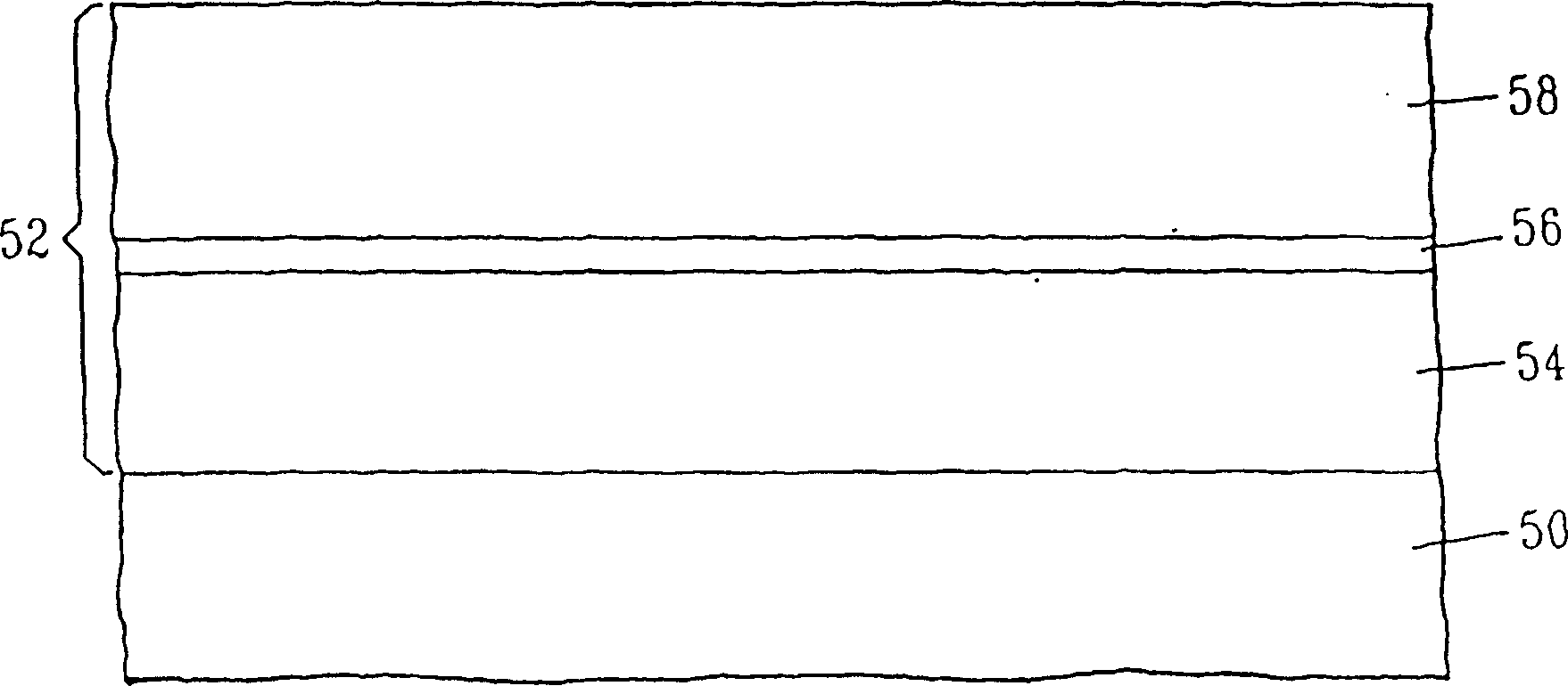
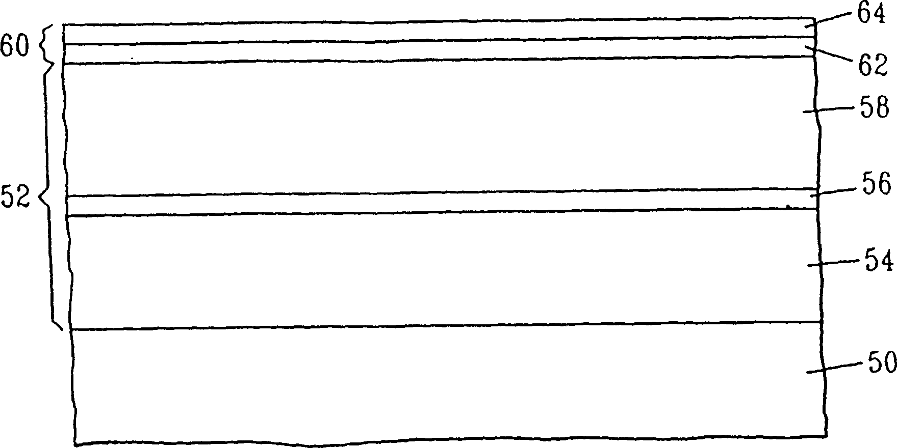
[0058]In this example, a SiLK(R) / HOSP / SiLK(R) / HOSP dielectric stack was prepared and used to form an interconnect structure. Specifically, in this example, a bare 8-inch Si wafer was used as the substrate. This wafer was treated with the adhesion promoter by applying a 2.5 weight percent solution of organosilane adhesion promoter in propylene glycol monomethyl ether acetate (PGMEA) to the wafer, followed by spinning at approximately 3000 rpm for 30 seconds . The wafer is then placed on a hot plate and baked at about 100 degrees Celsius for about 90 seconds. This bake promotes the reaction of the adhesion promoter to the surface of the wafer. After cooling to room temperature, the wafer with adhesion promoter was rinsed with propylene glycol monomethyl ether acetate (PGMEA) to remove excess adhesion promoter. The wafer was washed with about 30 milliliters (ml) of propylene glycol monomethyl ether acetate (PGMEA) and then spun at about 3000 rpm for about 30 seconds.

[0059]...


PUM

PropertyMeasurementUnit
sizeaaaaaaaaaa
sizeaaaaaaaaaa
thicknessaaaaaaaaaa

Abstract

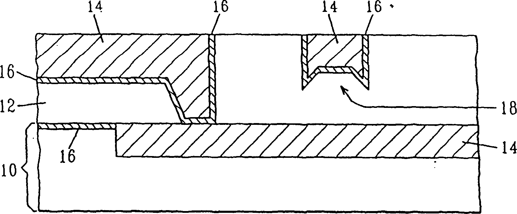
A low-k dielectric metal conductor interconnect structure having no micro-trenches present therein and a method of forming such a structure are provided. Specifically, the above structure is achieved by providing an interconnect structure which includes at least a multilayer of dielectric materials which are applied sequentially in a single spin apply tool and then cured in a single step and a plurality of patterned metal conductors within the multilayer of spun-on dielectrics. The control over the conductor resistance is obtained using a buried etch stop layer having a second atomic composition located between the line and via dielectric layers of porous low-k dielectrics having a first atomic composition. The inventive interconnect structure also includes a hard mask which assists in forming the interconnect structure of the dual damascene-type. The first and second composition are selected to obtain etch selectivity of at least 10 to 1 or higher, and are selected from specific groups of porous low-k organic or inorganic materials with specific atomic compositions and other discoverable quantities.

Description

technical field [0001] This invention relates to interconnect structures for high speed microprocessors, application specific integrated circuits (ASICs), and other high speed integrated circuits (ICs). The present invention provides low dielectric constant (ie, low-k) interconnect structures with enhanced circuit speed, precise conduction resistance values, and reduced manufacturing costs. The structure of the present invention has a lower effective dielectric constant, improved control of metal line resistance, and reduced manufacturing cost compared to conventional structures of the prior art. Background technique [0002] A number of low-k dielectrics with a dielectric constant of about 3.5 or less are known, plus dual damascene copper (Cu) interconnect structures, see, for example, Electrical and Electronic Engineers, 5-7 June 2000 Institute of Electronics (IEEE) Electron Devices Society, International Symposium on Interconnection Technology, R.D. Goldblatt, et al., "H...

Claims


Application Information

Patent Timeline
Patent Type & Authority Applications(China)
IPC IPC(8): H01L21/768H01L23/522H01L23/532
CPCH01L2924/0002H01L21/76811H01L21/76835H01L23/5329H01L23/5222H01L2924/00H01L21/28
Inventor S·M·盖茨J·C·赫德里克S·V·尼塔S·普鲁肖特哈曼C·S·蒂贝格
Owner GLOBALFOUNDRIES INC
Learn More