Semiconductor integrated circuit device and method for designing the same
A technology of integrated circuits and design methods, applied in the direction of semiconductor devices, circuits, semiconductor/solid-state device components, etc., can solve the problems of voltage reduction, difficulty in reducing power consumption of semiconductor integrated circuit devices, and difficulty in high-speed operation of semiconductor integrated circuit devices. , to achieve the effect of low power consumption design
- Summary
- Abstract
- Description
- Claims
- Application Information
AI Technical Summary
Problems solved by technology
Method used
Image

Examples
no. 1 Embodiment approach
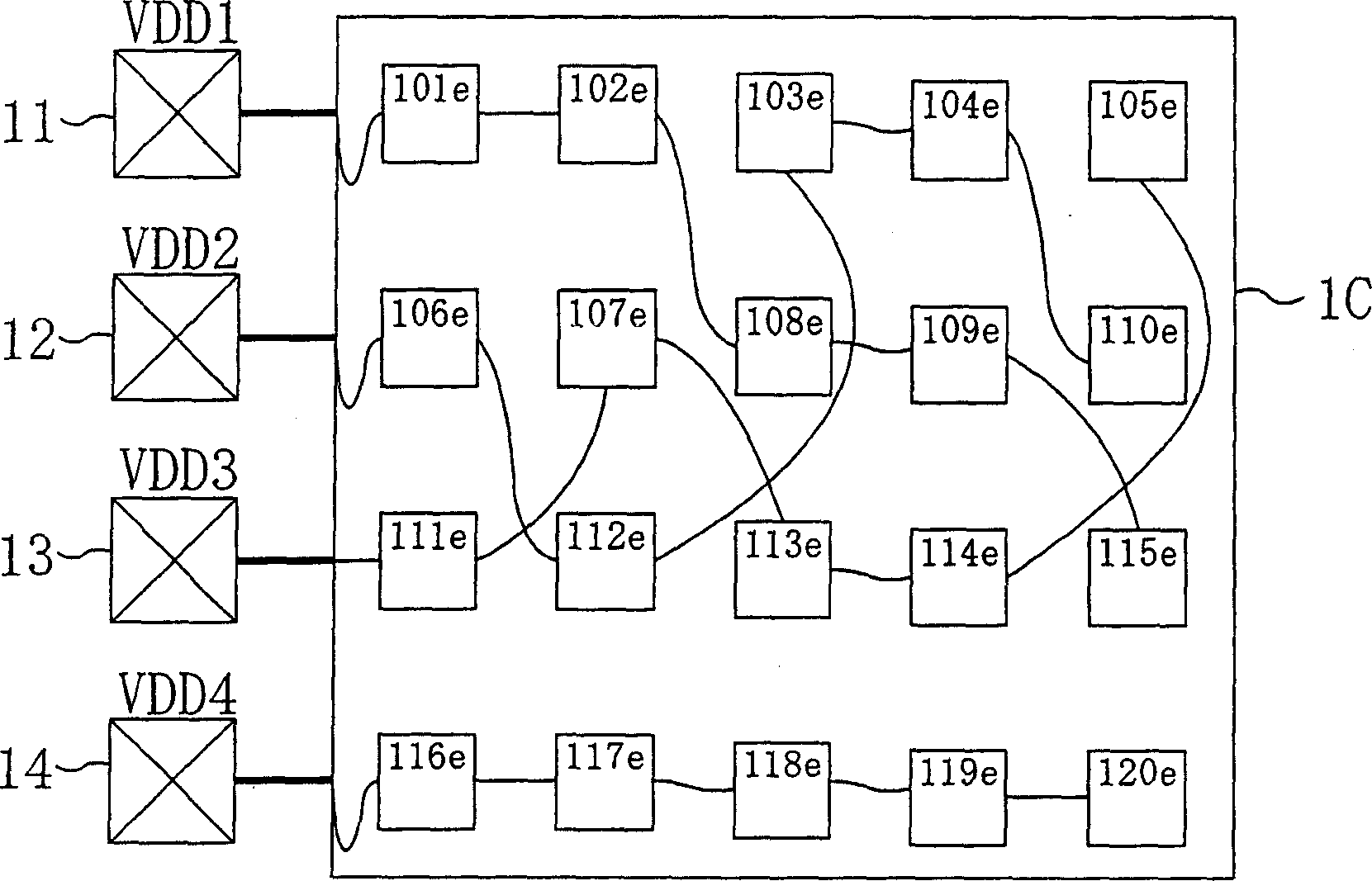
[0092] figure 1 A configuration example of the semiconductor integrated circuit device according to the first embodiment of the present invention is shown. exist figure 1In the shown semiconductor integrated circuit device, a circuit block 1C and power supplies 11 to 14 are shown.
[0093] The circuit block 1C has elements (hereinafter referred to as "components") 101e to 120e constituting the block 1C, and to the components 101e to 120e, any one of voltages VDD1 to VDD4 is supplied from power sources 11 to 14 (the Thick solid line). In addition, in figure 1 Here, the constituent elements 101e to 120e are connected by vias as shown in the figure. In addition, here, a circuit block refers to a block including a circuit of constituent elements such as an AND gate and an OR gate, for example.
[0094] The voltages VDD2 to VDD4 supplied to the circuit block 1C are voltages stepped down by a certain ratio based on the rated voltage VDD1 of the semiconductor integrated circuit ...
no. 2 Embodiment approach
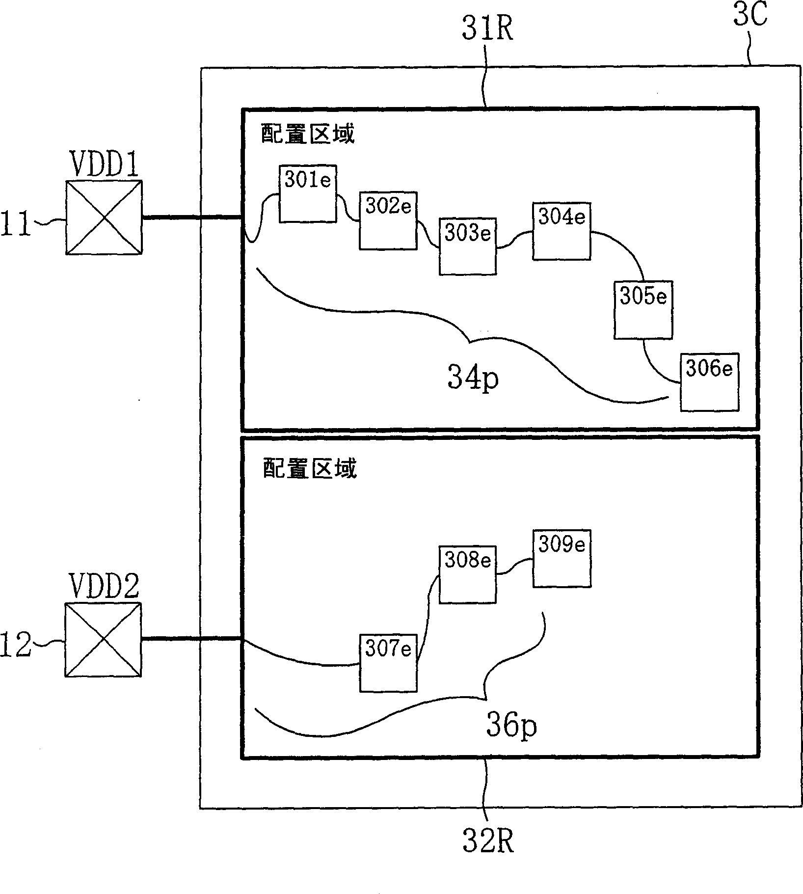
[0104] Hereinafter, in the second embodiment, as one of the methods for reducing power consumption by supplying individual power supply voltages to each component constituting the circuit block, a method is performed in a region determined in units of voltage (hereinafter referred to as The method of arranging each component in the arrangement area) will be described.
[0105] image 3 A configuration example of the semiconductor integrated circuit device according to the second embodiment of the present invention is shown.
[0106] Such as image 3 As shown, a layout region 31R and a layout region 32R are provided in the circuit block 3C, the voltage VDD1 from the power supply 11 is supplied to the layout region 31R, and the voltage VDD2 from the power supply 12 is supplied to the layout region 32R. Moreover, the component elements 301e-306e belonging to the route 34p are included in the layout area 31R, and the component elements 307e-309e belonging to the route 36p are in...
no. 3 Embodiment approach
[0115] Hereinafter, in the third embodiment, a method for realizing low power consumption in consideration of a voltage drop due to the IR-Drop effect will be described.
[0116] Figure 5 Shown is a configuration example of a semiconductor integrated circuit device according to a third embodiment of the present invention. As an example of the layout region described in the second embodiment, the voltage drop caused by the IR-Drop effect or the like occurring inside the layout region is considered. The configuration diagram of the interior of the configuration area.
[0117] Such as Figure 5 As shown, the power supply line 51L supplying the voltage VDD51 is arranged in the center of the arrangement region 50R, and a voltage drop due to the IR-Drop effect or the like occurs in the arrangement region 50R. For example, if the lower half of the configuration region 50R is used for illustration, the region with the shortest distance from the power supply wiring 51L is the region...
PUM
 Abstract
Description
Claims
Application Information
 - Generate Ideas
- Intellectual Property
- Life Sciences
- Materials
- Tech Scout
- Unparalleled Data Quality
- Higher Quality Content
- 60% Fewer Hallucinations
Browse by: Latest US Patents, China's latest patents, Technical Efficacy Thesaurus, Application Domain, Technology Topic, Popular Technical Reports.
© 2025 PatSnap. All rights reserved.Legal|Privacy policy|Modern Slavery Act Transparency Statement|Sitemap|About US| Contact US: help@patsnap.com