Method for mfg. semiconductor device

A manufacturing method, semiconductor technology, applied in semiconductor/solid-state device manufacturing, electrical components, circuits, etc., can solve problems such as uneven heating temperature, high price, difficult heat treatment temperature, etc.

Inactive Publication Date: 2004-02-18
PANASONIC CORP
View PDF0 Cites 0 Cited by
  • Summary
  • Abstract
  • Description
  • Claims
  • Application Information

AI Technical Summary

Problems solved by technology

[0014] In the latest semiconductor devices, there are cases where the process temperature treatment time of the rapid thermal process (RTP) is less than 10 seconds, and there are also cases where peak annealing is added to the instantaneous maximum temperature heat treatment. In such cases, the above heating temperature does not Uniformity is a fatal problem
[0015] In order to prevent such a bad situation, there are methods such as improving the low temperature controllability by using light from a visible light source, or changing the structure of the pyrometer or the heat treatment chamber of the rapid thermal process (RTP) device, but the device itself is expensive, or It is difficult to cope with the heat treatment temperature with large temperature changes, so it is not a very effective countermeasure

Method used


Image

  • Method for mfg. semiconductor device
  • Method for mfg. semiconductor device
  • Method for mfg. semiconductor device

Examples


no. 1 approach

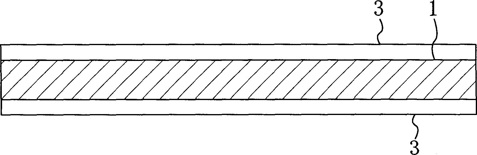
[0053] Figure 1(a) to Figure 1(c) , is a partial sectional view showing the semiconductor device manufacturing method according to the first embodiment of the present invention.

[0054] In the process shown in FIG. 1(a), first, a silicon semiconductor substrate 1 is prepared. Next, silicon oxide films are formed on the upper and lower surfaces of the substrate 1 by vapor phase deposition (CVD) or the like.

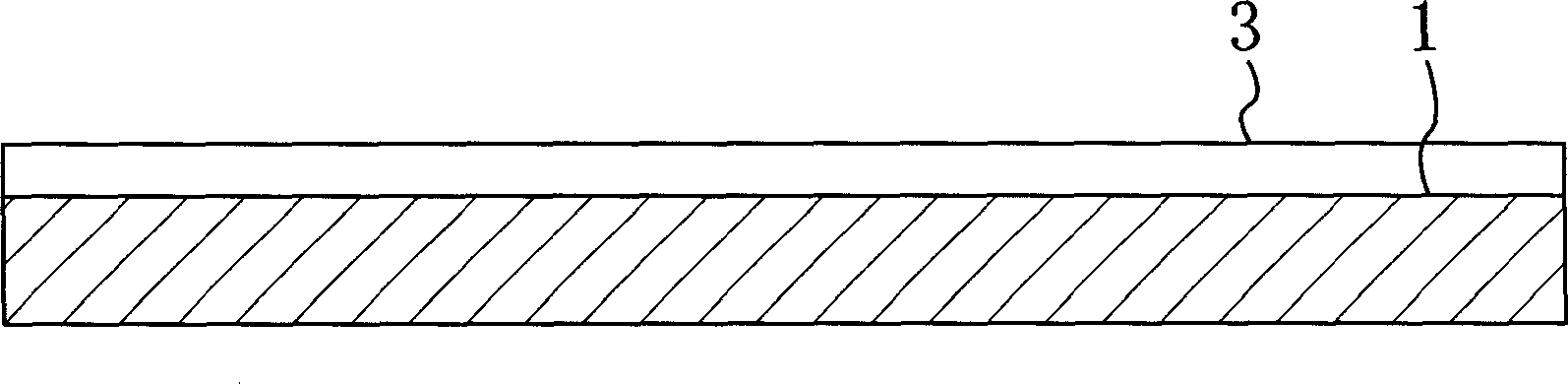
[0055] Next, in the process shown in FIG. 1(b), silicon oxide film 3 on the lower surface (back surface) of semiconductor substrate 1 is removed by wet etching.

[0056] Next, in the process shown in Figure 1(c), the substrate is placed on POCl 3 In a gas environment, it is heated to 850° C., and phosphorus (P) is implanted into the lower part of the semiconductor substrate 1 by means of heat conduction. As a result, the lower portion of the semiconductor substrate 1 is formed with a thickness of more than 3 μm and an average concentration of 3×10 18 cm -3 The above...

no. 2 approach

[0085] In the method of manufacturing a semiconductor device according to the second embodiment of the present invention, the method of forming the free carrier absorbing layer is different from that of the first embodiment. Below, it will be explained with reference to the figure.

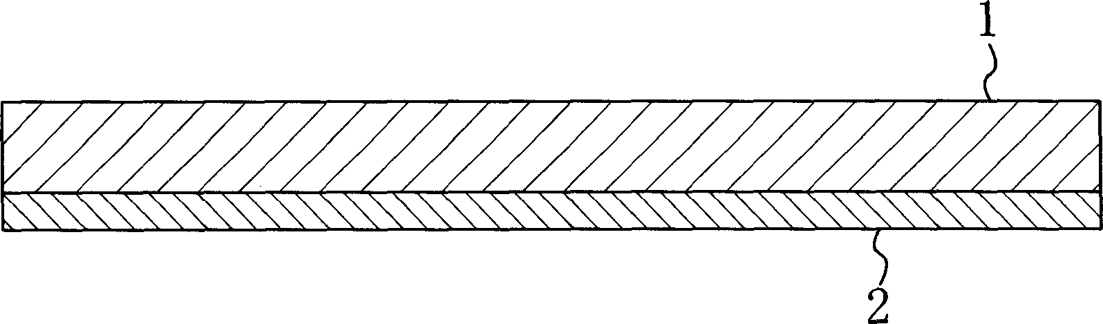
[0086] 5(a) and 5(b) are partial cross-sectional views showing a semiconductor device manufacturing method according to a second embodiment of the present invention.

[0087] First, in the process shown in FIG. 5( a ), N-type impurities are implanted into a region deeper than 3 μm from the upper surface of semiconductor substrate 1 by ion implantation. Thus, an average impurity concentration of 3×10 18 cm -3 Above, the free carrier absorbing layer 2 having a thickness of 3 μm or more. Thereafter, the semiconductor device is fabricated on the semiconductor substrate 1 .

[0088] Also, rapid thermal (RTP) processing is performed in the manufacturing process of the semiconductor device. In this ...


PUM


Abstract

Provided is a method for manufacturing a semiconductor device which can reduce variations of temperature in a wafer surface at a low cost, by improving the temperature controllability of an RTP. In a step for performing thermal treatment by subjecting the semiconductor substrate with a lamp light irradiation, a free carrier absorption layer for absorbing the irradiated lamp light is provided, in advance, in the semiconductor substrate. Thus, it is possible to increase the temperature controllability in a low temperature range during RTP process, and to reduce, at a low cost, variations in the substrate temperature, not only in a low temperature range but also in a processing temperature range. As a result, semiconductor devices that require precise thermal treatment can be manufactured, without deteriorating the characteristics of the resulting semiconductor devices.

Description

technical field [0001] The invention relates to a manufacturing method of a semiconductor device, in particular to a manufacturing method of a semiconductor device heat-treated with infrared rays. Background technique [0002] In the case of manufacturing semiconductor devices on a wafer of a silicon substrate, it is necessary to implant impurities into the wafer by methods such as ion implantation, vapor phase growth, and solid diffusion, and perform thermal diffusion by high-temperature annealing. In the heat treatment process of such a semiconductor device, it is necessary to set appropriate treatment conditions and perform appropriate heat treatment on the wafer. [0003] As a typical method of thermally treating a wafer conventionally used, rapid thermal processing (RTP=Rapid Thermal Processing) is exemplified. This is a possible lighting method for high temperature and short time treatment. In a rapid thermal (RTP) device, generally, a Tungsten Halogen Lamp (Tungsten...

Claims


Application Information

Patent Timeline
Patent Type & Authority Applications(China)
IPC IPC(8): H01L21/265H01L21/26H01L21/268H01L21/324
CPCH01L21/324H01L21/2686
Inventor 庭山雅彦米田健司
Owner PANASONIC CORP
Why Eureka
Try Eureka