Method for forming metal silicide in shielded read-only memory

A metal silicide, read-only memory technology, used in semiconductor/solid-state device manufacturing, electrical components, circuits, etc., can solve difficulties, limit the application of metal silicide, and cannot form metal silicide.

Inactive Publication Date: 2004-02-04
GRACE SEMICON MFG CORP
View PDF0 Cites 3 Cited by
  • Summary
  • Abstract
  • Description
  • Claims
  • Application Information

AI Technical Summary

Problems solved by technology

However, the self-aligned metal silicide process requires additional steps in the manufacturing process
In addition, the structure of some components will limit the application of metal silicide, for example, embedded (embed) shielded read-only memory, considering the problem of leakage current, buried in the memory cell (memory cell storage unit) ) heavily doped region, metal silicide cannot be formed
Known metal silicide process steps are difficult to form such components

Method used


Image

  • Method for forming metal silicide in shielded read-only memory
  • Method for forming metal silicide in shielded read-only memory
  • Method for forming metal silicide in shielded read-only memory

Examples


Embodiment Construction

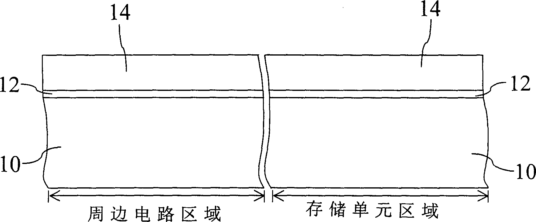
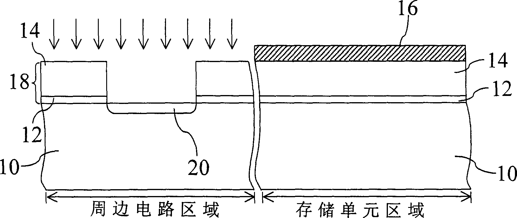
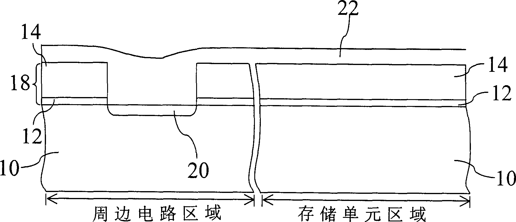
[0010] The semiconductor design of the present invention can be widely applied in many semiconductor designs, and can utilize many different semiconductor materials to make, when the present invention illustrates the method of the present invention with a preferred embodiment, those who know this field should have It is recognized that many steps can be changed, and materials and impurities can also be replaced, and these general replacements undoubtedly do not depart from the spirit and scope of the present invention.

[0011] Secondly, the present invention is described in detail with schematic diagrams as follows. When describing the embodiments of the present invention in detail, the cross-sectional view showing the semiconductor structure will not be partially enlarged according to the general scale in the semiconductor manufacturing process for the convenience of explanation, but it should not be used as a limited definition. Know. In addition, in actual production, the ...


PUM


Abstract

The method includes the following steps: providing a semiconductor structure with defined peripheral circuit region and storage unit region as the storage unit region having a buried doping zone, forming a polysilicon layer on the semiconductor structure to remove partial polysilicon layer to form at least one grid at peripheral circuit region, forming a gap wall at sidewall of grid and a metal silicide on grid and polysilicon layer and removing partial metal silicide and polysilicon layer at storage unit region to expose buried doping zone on it.

Description

【Technical field】 [0001] The present invention relates to a method for forming metal silicide in a semiconductor device, and more particularly to a method for forming metal silicide in a mask ROM (mask ROM). 【Background technique】 [0002] Traditional masked ROMs include NOR-type and NAND-type. The NOR-type shielded ROM is formed by connecting the source and the drain of the memory transistor in parallel. Another type of NAND-type shielded ROM that connects the source and drain of memory transistors in series. However, due to the miniaturization of components, the traditional ROM encounters the problem of increased impedance of wordlines and bitlines due to reduced line width. The increased impedance of the ROM device affects the operating speed of the device. [0003] One of the methods to solve the high impedance is to use thin metal silicide (silicide) to reduce the impedance of the word line and the bit line. Compared with the non-metal silicide structure, the metal ...

Claims


Application Information

Patent Timeline
Patent Type & Authority Applications(China)
IPC IPC(8): H01L21/8246
Inventor 叶双凤
Owner GRACE SEMICON MFG CORP
Why Eureka
Try Eureka