


Quick Research
Generate reliable direction feasibility study reports for your R&D in just a few steps.

Technical Q&A
Discover and master advanced knowledge NOW. Basics, ideas, possibilities, all at once.

Find Solutions
As an expert in R&D theories, this can generate solutions to your technical problems instantly.

Evaluate Feasibility
Analyze your overall solution with one click, know your potential R&D risks in advance.

Monitor Landscape
Get weekly tech updates, stay abreast of the latest tech innovations and key insights.
Improved mask ROM process and element
A read-only memory, mask-type technology, applied in electrical components, electrical solid-state devices, semiconductor devices, etc., can solve the problems of the initial voltage drop of memory cells, improper reading of memory cells, etc., to achieve high component yield, easy effect used
- Summary
- Abstract
- Description
- Claims
- Application Information
AI Technical Summary
Problems solved by technology
Method used
Image

Examples
Embodiment Construction
[0015] The present invention provides techniques including methods of manufacturing semiconductor elements. More specifically, the present invention provides a method for manufacturing a masked ROM, which can reduce its critical dimension and effectively avoid the breakdown effect. However, the scope of application of the present invention is wider than this. For example, the present invention can be applied to the design of embedded ROM and other aspects.
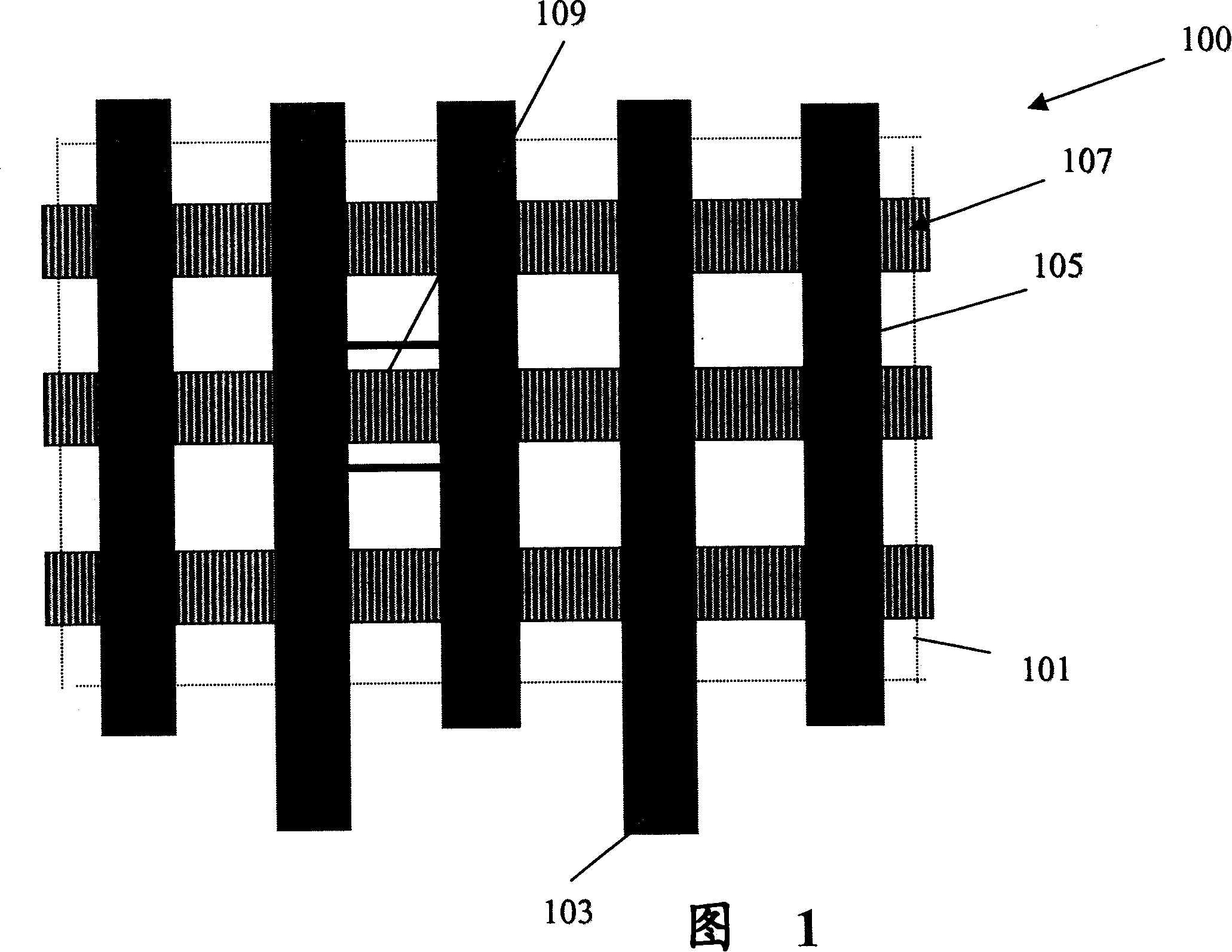
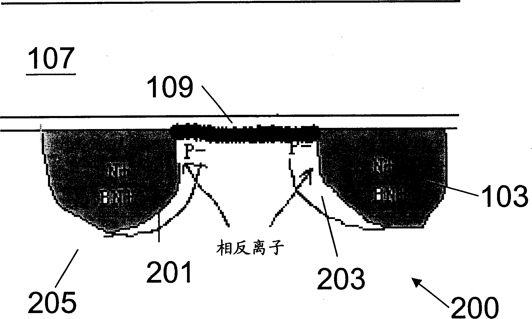
[0016] FIG. 1 shows a top view 100 of a masked ROM cell design in accordance with an embodiment of the present invention. This figure is only an example and should not be used to limit the scope of this patent application. Any person skilled in the art will understand that the present invention can have many other variations, modifications and applications. As shown, the top view includes a plurality of polysilicon conductors 107 each defining a word line for a memory cell array 101 . Source / drain regions or active reg...
PUM
 Abstract
Description
Claims
Application Information
 - R&D Engineer
- R&D Manager
- IP Professional
- Industry Leading Data Capabilities
- Powerful AI technology
- Patent DNA Extraction
Browse by: Latest US Patents, China's latest patents, Technical Efficacy Thesaurus, Application Domain, Technology Topic, Popular Technical Reports.
© 2024 PatSnap. All rights reserved.Legal|Privacy policy|Modern Slavery Act Transparency Statement|Sitemap|About US| Contact US: help@patsnap.com