Light emitting semiconductor chip and method for producing light emitting semiconductor chip

A technology of light-emitting semiconductors and semiconductors, which is applied in the field of light-emitting semiconductor chips and used in the manufacture of light-emitting semiconductor chips, and can solve problems such as consumption, reduced output, and high logistics

Active Publication Date: 2021-12-28
OSRAM OPTO SEMICON GMBH & CO OHG
View PDF7 Cites 0 Cited by
  • Summary
  • Abstract
  • Description
  • Claims
  • Application Information

AI Technical Summary

Problems solved by technology

[0005] For the above-mentioned applications, different laser diodes with correspondingly different emission wavelengths are usually selected, which however leads to high logistical expenditure and reduced yields due to rejects of laser diodes with unsuitable wavelengths

Method used


Image

  • Light emitting semiconductor chip and method for producing light emitting semiconductor chip
  • Light emitting semiconductor chip and method for producing light emitting semiconductor chip
  • Light emitting semiconductor chip and method for producing light emitting semiconductor chip

Examples


Embodiment Construction

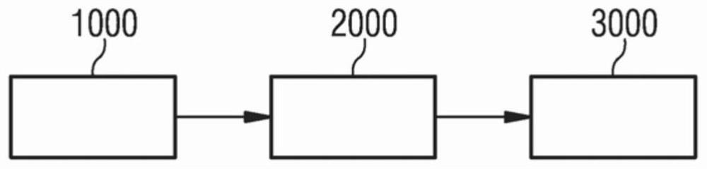
[0060] exist figure 1 A method for producing a light-emitting semiconductor chip according to an exemplary embodiment is shown in , wherein a semiconductor chip having a first semiconductor layer having a lateral variation of the material composition is produced. To this end, in a first method step 1000 , a surface is provided on which a first semiconductor layer is grown. The first semiconductor layer can preferably be part of a semiconductor layer sequence which, besides the first semiconductor layer, has a plurality of further semiconductor layers. The surface provided for growing the first semiconductor layer can be formed by a growth substrate or a semiconductor layer grown on the growth substrate, which can also be part of an already grown sublayer stack of the semiconductor layer sequence.

[0061] In a further method step 2000 a first semiconductor layer sequence is grown on the provided surface. This can also mean that one or more further semiconductor layers of the...


PUM

PropertyMeasurementUnit
sizeaaaaaaaaaa

Abstract

A light-emitting semiconductor chip (100) is proposed having a first semiconductor layer (1) which is at least part of an active layer provided for generating light and which has a material composition along at least one direction of extension horizontal changes. Furthermore, a method for producing a semiconductor chip (100) is proposed.

Description

[0001] Cross References to Related Applications [0002] This application claims priority from German patent application 10 2016 108 892.7, the disclosure content of which is hereby incorporated by reference. technical field [0003] A light-emitting semiconductor chip and a method for producing a light-emitting semiconductor chip are proposed. Background technique [0004] For many laser-based applications, such as projection applications, suitable laser diodes emitting at multiple wavelengths, where the wavelengths vary in a defined manner, are lacking. Furthermore, it would be very advantageous for laser projection that the laser source be able to produce slightly varying wavelengths in order thereby to reduce the appearance of speckle patterns. Laser sources with different wavelengths are also required for message transmission by means of wavelength multiplexing and in biosensing technology. [0005] For the above-mentioned applications, different laser diodes with cor...

Claims


Application Information

Patent Timeline
Patent Type & Authority Patents(China)
IPC IPC(8): H01S5/323H01S5/343H01L33/08H01L33/28H01L33/30H01L33/32H01L33/00
CPCH01L33/0062H01L33/0083H01L33/08H01L33/28H01L33/30H01L33/32H01S5/32308H01S5/34333H01L33/0095H01L33/325H01L21/02458H01L21/0254H01L21/02617H01S5/026H01S5/1053H01S5/22H01S5/32341H01S2304/00H01S5/4087H01L27/153H01L33/0075H01S5/1096H01S5/3013H01L33/0025
Inventor 克里斯托夫·艾希勒安德烈·佐默斯贝恩哈德·施托耶茨安德烈亚斯·莱夫勒艾尔弗雷德·莱尔
Owner OSRAM OPTO SEMICON GMBH & CO OHG
Why Eureka
Try Eureka