Multi electric potential field plate lateral high voltage N type MOS transistor

A field plate and multi-potential technology, which is applied in the direction of semiconductor devices, circuits, electrical components, etc., can solve the problems of increasing the peak electric field of the drain region, reducing the reliability of the chip, and improving the breakdown voltage, so as to improve the breakdown voltage, Effect of reducing impact ionization and reducing on-resistance

Inactive Publication Date: 2007-07-04
SOUTHEAST UNIV
View PDF6 Cites 0 Cited by
  • Summary
  • Abstract
  • Description
  • Claims
  • Application Information

AI Technical Summary

Problems solved by technology

It is precisely because of the continuous expansion of related application fields that various structures of high-voltage N-type metal oxide semiconductor devices have appeared, especially the field plate structure has been widely used, but the field plate structure also brings a problem, that is, The electric field at the end of the field plate is very high, which limits the further improvement of the breakdown voltage of the high-voltage NMOS device. The multi-field plate structure can alleviate this phenomenon, but it will also increase the peak electric field of the drain region. It leads to the reduction of the safe working area of ​​high-voltage N-type metal-oxide-semiconductor devices during high-current output, and reduces the reliability of the chip

Method used


Image

  • Multi electric potential field plate lateral high voltage N type MOS transistor

Examples


Embodiment

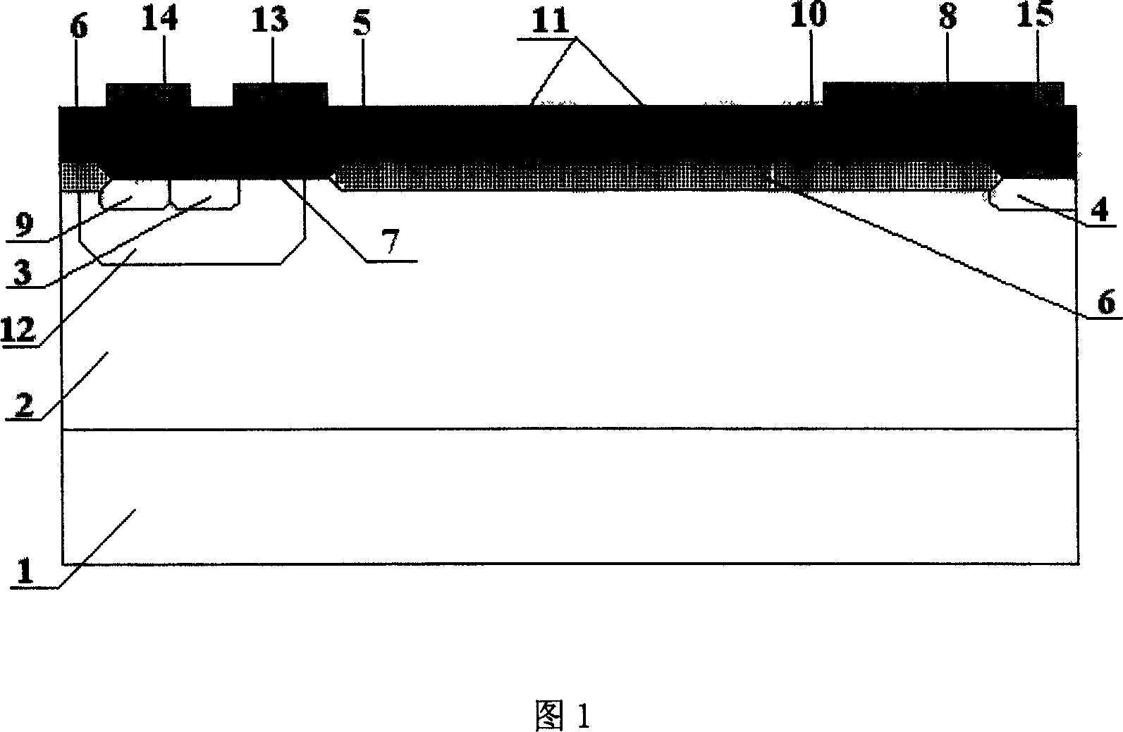
[0015] Embodiment A multi-potential field plate high-voltage N-type metal oxide semiconductor transistor involving a high-voltage device is composed of an N-type substrate 1, a P-type epitaxial layer 2, a source 3, a drain 4, a polysilicon gate 5, a field oxide layer 6 and The P-type epitaxial layer 2 is set on the top of the N-type substrate 1, the field oxide layer 6 is located between the source 3 and the drain 4, and the source 3, drain 4, polysilicon gate 5 and field oxide layer 6 are located on the P-type Above the epitaxial layer 2, a gate oxide layer 7 is provided between the polysilicon gate 5 and the P-type epitaxial layer 2, and the oxide layer 8 is located above the source 3, the drain 4, the polysilicon gate 5 and the field oxide layer 6, and the P-type epitaxial layer A P-type contact hole 9 is provided above the layer 2, below the oxide layer 8 and between the source 3 and the field oxide layer 6, and metal aluminum leads 13, 14 and 15 are respectively provided o...


PUM


Abstract

Disclosed relates to multi electric potential field electrode plate high-pressured N-typed metal oxide semiconductor of high-voltaged component, comprising N-typed substrate, P-typed epitaxial layer, source and drain, multi- silicon polycrystal, field oxide layer and oxide layer, silicon polycrystal field electrode plate above field oxide layer and between drain and silicon polycrystal gate , which is connected to drain. The invention brings in silicon polycrystal field electrode plate with the same electric potential of drain end, which makes the surface of floating area deviation area below silicon polycrystal field electrode plate in accumulation condition of current carrier, greatly reducing peak electric field between drain end and silicon polycrystal field electrode plate when in operation work condition and impact ionization of current carrier on drain end, so Kirk effect(the effect of breakdown voltage reduction caused by electric field accumulating under large current ) is notably decreased, breakdown voltage and area of safe operation are increased.

Description

technical field [0001] The invention is a metal oxide semiconductor tube, especially a multi-potential field plate high-voltage N-type metal oxide semiconductor tube. Background technique [0002] Metal-oxide-semiconductor high-voltage devices have the advantages of good switching characteristics and low power consumption. More importantly, metal-oxide-semiconductor high-voltage devices are easily compatible with standard low-voltage metal-oxide-semiconductor processes and reduce chip production costs. Metal oxide semiconductor high-voltage integrated devices have absolute advantages in the application range of 600V. Within the working voltage of 100V, the use of bulk silicon materials has the advantage of low cost, but above 100V, bulk silicon materials can no longer meet the design requirements. Therefore, epitaxial materials It will become the first choice, and the use of epitaxial materials can meet the working voltage requirements within 1000V....

Claims


Application Information

Patent Timeline
Patent Type & Authority Patents(China)
IPC IPC(8): H01L29/78
Inventor 孙伟锋陆生礼吴建辉易扬波宋慧滨时龙兴
Owner SOUTHEAST UNIV
Why Eureka
Try Eureka