Susceptor for semiconductor manufacturing equipment and process for producing the same
A technology for holding bodies and silicon wafers, which is applied in semiconductor/solid-state device manufacturing, manufacturing tools, chemical instruments and methods, etc., and can solve problems such as the impossibility of obtaining dense products and difficulties in sintering
- Summary
- Abstract
- Description
- Claims
- Application Information
AI Technical Summary
Problems solved by technology
Method used
Image

Examples
example 1
[0045] AlN powder having an average particle size of 0.8 μm, an oxygen content of 1% by weight and a cationic impurity content of not more than 0.3% by weight; yttrium oxide powder and yttrium stearate powder having an average particle size of 0.3 μm, as a sintering aid; and PVB as an organic binder. Weigh AlN powder and sintering aid powder in this way, as shown in Table 1, replace the total amount of sintering aid with the weight of Y element, and the rest is AlN by weight. As an organic binder, 3% by weight of PVB based on their total weight (100% by weight) was weighed. Then, they were mixed in an ethanol solution with nylon balls using a ball mill in an alumina tank over 12 hours. The resulting slurry was spray-dried and granulated into substantially round granules, wherein the proportion of particles with an average particle size of 80 μm was about 20% by weight, and the proportion of particles with an average particle size of 200 μm was about 20% by weight. 80% of (gr...
example 2
[0062] The same AlN powder as in Example 1 was prepared, and as a sintering aid, yttrium oxide had an average particle size of 0.4 μm, neodymium oxide powder had an average particle size of 0.3 μm, lanthanum oxide powder had an average particle size of 0.3 μm and calcium oxide powder had an average particle size of 0.3 μm; and PVB as an organic binder. The AlN powder and the sintering aid were weighed in such a manner that the weight of the sintering aid was shown in Table 5 in terms of the respective elements, and the total amount thereof was 0.8 parts by weight, and the remainder was AlN. And, as organic, PVB was weighed as 10% based on its total amount (100%). They were mixed with nylon balls in ethanol solvent in the alumina tank of the ball mill for 12 hours. The resulting slip was spray dried. Granulated substantially round granule state in which about 20% by weight of granules with an average particle size of 70 μm and about 78% by weight of granules with an average p...
example 3
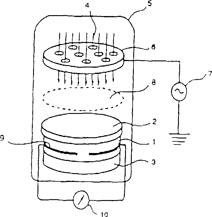
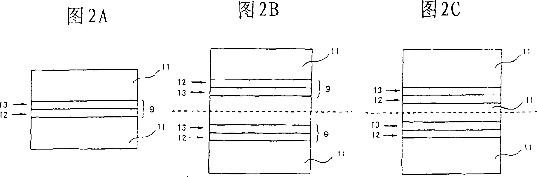
[0067] Using trimmed substrates or substrate samples of the molded body of Example 1, holders were fabricated for testing by laminating multiple sheets of these samples. For lamination into these substrate samples with the material of the intercalation layer, a high-melting-point metal layer to which the low-melting-point glass composition shown in Table 6 was added and a conductive paste containing various compositions shown in Table 7 were prepared. The values in Table 6 are the weight of each high-melting-point metal layer in the conductive adhesive after the volatile components are discharged during sintering, while the rest of the high-melting-point metal, that is, W, Mo and Ta is basically the total amount of glass components . Therefore, in the case of sample b of this example, the total amount of the glass component in the refractory metal layer is 50% by weight.
[0068] insert layer
the symbol
Composition and content (weight% of content)
Rati...
PUM
| Property | Measurement | Unit |
|---|---|---|
| Diameter | aaaaa | aaaaa |
| Warpage | aaaaa | aaaaa |
| Thickness | aaaaa | aaaaa |
Abstract
Description
Claims
Application Information
 - R&D
- Intellectual Property
- Life Sciences
- Materials
- Tech Scout
- Unparalleled Data Quality
- Higher Quality Content
- 60% Fewer Hallucinations
Browse by: Latest US Patents, China's latest patents, Technical Efficacy Thesaurus, Application Domain, Technology Topic, Popular Technical Reports.
© 2025 PatSnap. All rights reserved.Legal|Privacy policy|Modern Slavery Act Transparency Statement|Sitemap|About US| Contact US: help@patsnap.com