Preparation method of SERS (Surface Enhanced Raman Scattering) substrate with wettability multistage nano array structure
A nano-array and nano-structure technology, which is applied in the field of preparation of wettable multi-level nano-array structure SERS substrate, can solve the problems of poor repeatability measurement of SERS substrate signal and insufficient structure uniformity, so as to improve detection sensitivity and Enhancement Factors, High Sensitivity and Uniformity, Effect of Enhanced Degree of Control
- Summary
- Abstract
- Description
- Claims
- Application Information
AI Technical Summary
Problems solved by technology
Method used
Image
Examples
preparation example Construction
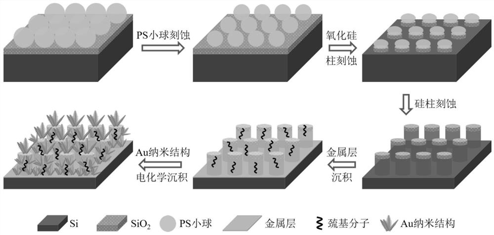
[0047] A preparation method of a wettable multi-level nano-array structure SERS substrate, such as figure 1 As shown, the method includes the following steps:
[0048] 1) Polish the silicon wafer containing the silicon oxide layer, clean it, and then use the gas-liquid interface self-assembly method to deposit a single-layer polystyrene (PS) ball in a hexagonal close arrangement on the surface of the silicon oxide as a subsequent etching mask ; Using low-temperature inductively coupled plasma-enhanced reactive ion etching (ICP-RIE) or plasma degumming technology to etch the obtained hexagonal close-arranged monolayer PS film, and each sphere is uniformly reduced to a specific size, to obtain a PS nanosphere mask layer with equal spacing and non-close arrangement;
[0049] 2) Reactive ion etching (RIE) technology is used to etch silicon oxide with polystyrene nanospheres as a mask to form a large-area ordered polystyrene-silicon oxide column array structure;
[0050] 3) conti...
Embodiment 1
[0054] 1) Use a 4-inch single-sided polished silicon wafer with a 300nm silicon oxide layer as the substrate, and configure concentrated H 2 SO 4 :H 2 O 2 Mix the cleaning solution, immerse the silicon wafer substrate in it, boil it at 120°C for 2 hours, remove oil stains and other contaminants on the surface of the silicon wafer, rinse with ultrapure water and rinse with N 2 Blow dry spare;
[0055] The cleaned wafers were placed in the apparatus mentioned in the work already reported by our group (doi: 10.1109 / NEMS51815.2021.9451289), deionized water was added to completely submerge the wafer, and 6 mL of 20 mM The SDS solution was allowed to stand for 10 min, and then 550 μL of PS suspension with a diameter of 300 nm (volume ratio, alcohol: PS=3:2) was added to the above solution very slowly along the slide with a micro-syringe, and allowed to stand for 1 h. The PS monolayer film on the gas-liquid interface was transferred to the silicon oxide wafer, and the spherical d...
Embodiment 2
[0064] The preparation method of the wettable multi-level nano-array structure SERS substrate of Example 2 is the same as that of Example 1, except that the thickness of silicon oxide selected in step 1) of Example 1 is 100 nm, and the silicon oxide in step 2) is etched The reactive gas used in the etching is CF 4 , the gas flow rate is 40sccm, the reaction pressure is 1Pa, the etching power is 300W, the etching time is 180s, and the silicon oxide etching depth is 100nm; the reaction gas used in the silicon etching in step 3) is SF 6 and O 2 , the gas flow is 60sccm and 10sccm, the reaction pressure is 5Pa, the etching power is 300W, the etching time is 420s, and the silicon etching depth is 600nm; in step 4), a chemical coupling method is used to load a Layers of gold nanoparticles.
PUM
| Property | Measurement | Unit |
|---|---|---|
| height | aaaaa | aaaaa |
| height | aaaaa | aaaaa |
| thickness | aaaaa | aaaaa |
Abstract
Description
Claims
Application Information
 - R&D
- Intellectual Property
- Life Sciences
- Materials
- Tech Scout
- Unparalleled Data Quality
- Higher Quality Content
- 60% Fewer Hallucinations
Browse by: Latest US Patents, China's latest patents, Technical Efficacy Thesaurus, Application Domain, Technology Topic, Popular Technical Reports.
© 2025 PatSnap. All rights reserved.Legal|Privacy policy|Modern Slavery Act Transparency Statement|Sitemap|About US| Contact US: help@patsnap.com


